
Flowable carbon for semiconductor processing

a technology of flowable carbon and semiconductors, applied in the direction of semiconductor/solid-state device testing/measurement, chemical vapor deposition coating, coating, etc., can solve the problem of difficult to fill gaps without dielectric materials, new challenges arise, and conventional chemical vapor deposition techniques often experience an overgrowth of materials

Active Publication Date: 2014-02-13
APPLIED MATERIALS INC
View PDF5 Cites 272 Cited by
  • Summary
  • Abstract
  • Description
  • Claims
  • Application Information

AI Technical Summary

Benefits of technology

The patent describes methods for creating carbon layers on silicon substrates using flowable precursors. The carbon layers can be deposited using a hot filament, plasma, or UV light. The resulting layers contain carbon-silicon bonds. The invention provides a way to create high-quality carbon layers on silicon wafers during semiconductor manufacturing.

Problems solved by technology

As the dimensions continue to get smaller, new challenges arise for process steps like filling a gap between circuit elements with a variety of materials.
As the width between the elements continues to shrink, the gap between them often gets taller and narrower, making the gap difficult to fill without the dielectric material getting stuck to create voids and weak seams.
Conventional chemical vapor deposition (CVD) techniques often experience an overgrowth of material at the top of the gap before it has been completely filled.
This can create a void or seam in the gap where the depositing dielectric material has been prematurely cut off by the overgrowth; a problem sometimes referred to as breadloafing.
While the deposition of flowable dielectric films deposited by CVD has fewer breadloafing problems, such techniques are still unavailable for some classes of material.

Method used


Image

  • Flowable carbon for semiconductor processing
  • Flowable carbon for semiconductor processing
  • Flowable carbon for semiconductor processing

Examples


Embodiment Construction

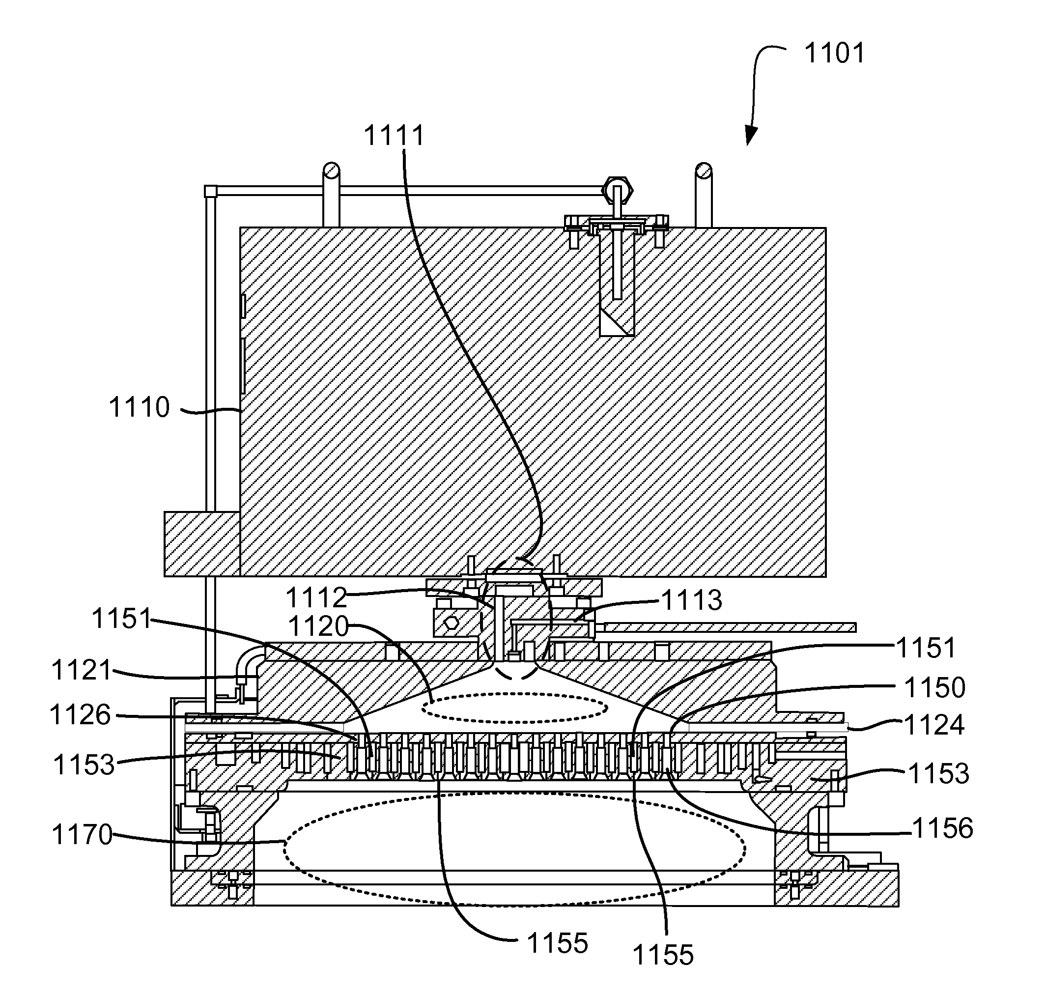
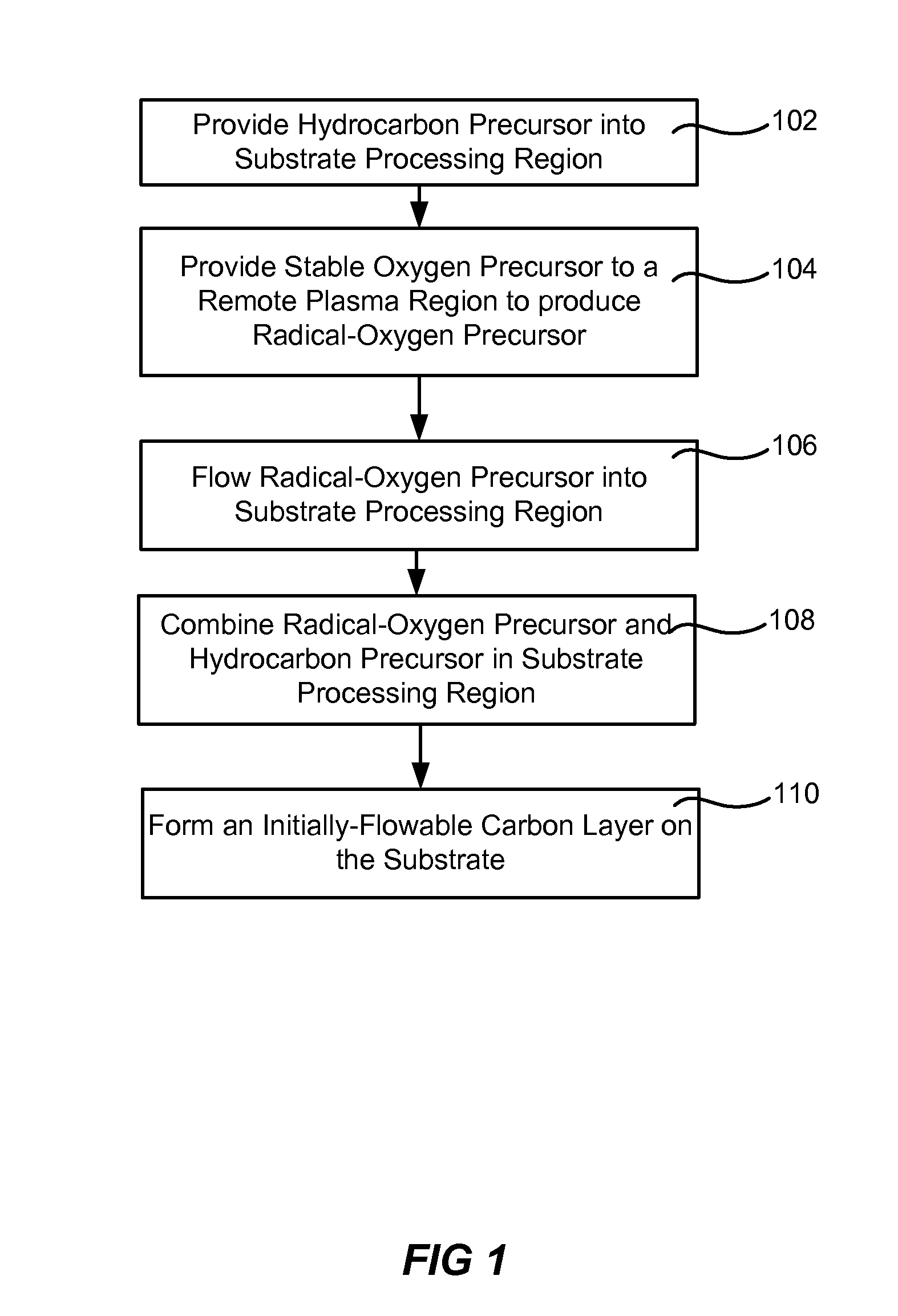
[0015]Methods are described for forming flowable carbon layers on a semiconductor substrate. A local excitation (such as a hot filament in hot wire CVD, a plasma in PECVD or UV light) may be applied as described herein to a silicon-free carbon-containing precursor containing a hydrocarbon to form a flowable carbon-containing film on a substrate. A remote excitation method has also been found to produce flowable carbon-containing films by exciting a stable precursor to produce a radical precursor which is then combined with unexcited silicon-free carbon-containing precursors in the substrate processing region.

[0016]In the case of a local excitation, a hot filament may be used to excite the silicon-free carbon-containing precursor in a deposition technique referred to as hot-wire chemical vapor deposition (HW-CVD). UV light or a local plasma may also be used to excite the silicon-free carbon-containing precursor. The inventors have determined that these techniques can be modified to f...


PUM

PropertyMeasurementUnit
temperatureaaaaaaaaaa
plasma poweraaaaaaaaaa

Abstract

Methods are described for forming flowable carbon layers on a semiconductor substrate. A local excitation (such as a hot filament in hot wire CVD, a plasma in PECVD or UV light) may be applied as described herein to a silicon-free carbon-containing precursor containing a hydrocarbon to form a flowable carbon-containing film on a substrate. A remote excitation method has also been found to produce flowable carbon-containing films by exciting a stable precursor to produce a radical precursor which is then combined with unexcited silicon-free carbon-containing precursors in the substrate processing region.

Description

CROSS-REFERENCES TO RELATED APPLICATIONS[0001]This application claims the benefit of U.S. Prov. Pat. App. No. 61 / 680,758 filed Aug. 8, 2012, and titled “FLOWABLE CARBON FOR SEMICONDUCTOR PROCESSING,” by Abhijit Basu Mallick et al., the entire disclosure of which is hereby incorporated herein in its entirety by reference for all purposes.STATEMENT AS TO RIGHTS TO INVENTIONS MADE UNDER FEDERALLY SPONSORED RESEARCH AND DEVELOPMENT[0002]NOT APPLICABLEREFERENCE TO A “SEQUENCE LISTING,” A TABLE, OR A COMPUTER PROGRAM LISTING APPENDIX SUBMITTED ON A COMPACT DISK[0003]NOT APPLICABLEBACKGROUND OF THE INVENTION[0004]The miniaturization of semiconductor circuit elements has reached a point where feature sizes of 45 nm, 32 nm, 28 nm and even 20 nm are fabricated on a commercial scale. As the dimensions continue to get smaller, new challenges arise for process steps like filling a gap between circuit elements with a variety of materials. As the width between the elements continues to shrink, the...

Claims


Application Information

Patent Timeline
Patent Type & Authority Applications(United States)
IPC IPC(8): H01L21/02
CPCH01L21/0226C23C16/26H01L21/02527H01L21/0262H01L21/02115H01L21/02274H01L21/02277H01L22/20H01L22/12H01L21/7682
Inventor MALLICK, ABHIJIT BASUINGLE, NITIN K.
Owner APPLIED MATERIALS INC
Learn More