Hard mask for patterning magnetic tunnel junctions

a tunnel junction and hard mask technology, applied in the manufacture/treatment of galvano-magnetic devices, magnetic field-controlled resistors, and details of galvano-magnetic devices, etc., can solve the problems of increasing the probability of device failure and reducing the yield of devices

Inactive Publication Date: 2016-12-01
APPLIED MATERIALS INC
View PDF6 Cites 78 Cited by
  • Summary
  • Abstract
  • Description
  • Claims
  • Application Information

AI Technical Summary

Problems solved by technology

As a result, etching of the MTJs becomes increasingly difficult and adjacent MTJs are insufficiently separated, which causes reduced device yield and increases the probability of device failure.

Method used


Image

  • Hard mask for patterning magnetic tunnel junctions
  • Hard mask for patterning magnetic tunnel junctions
  • Hard mask for patterning magnetic tunnel junctions

Examples


Embodiment Construction

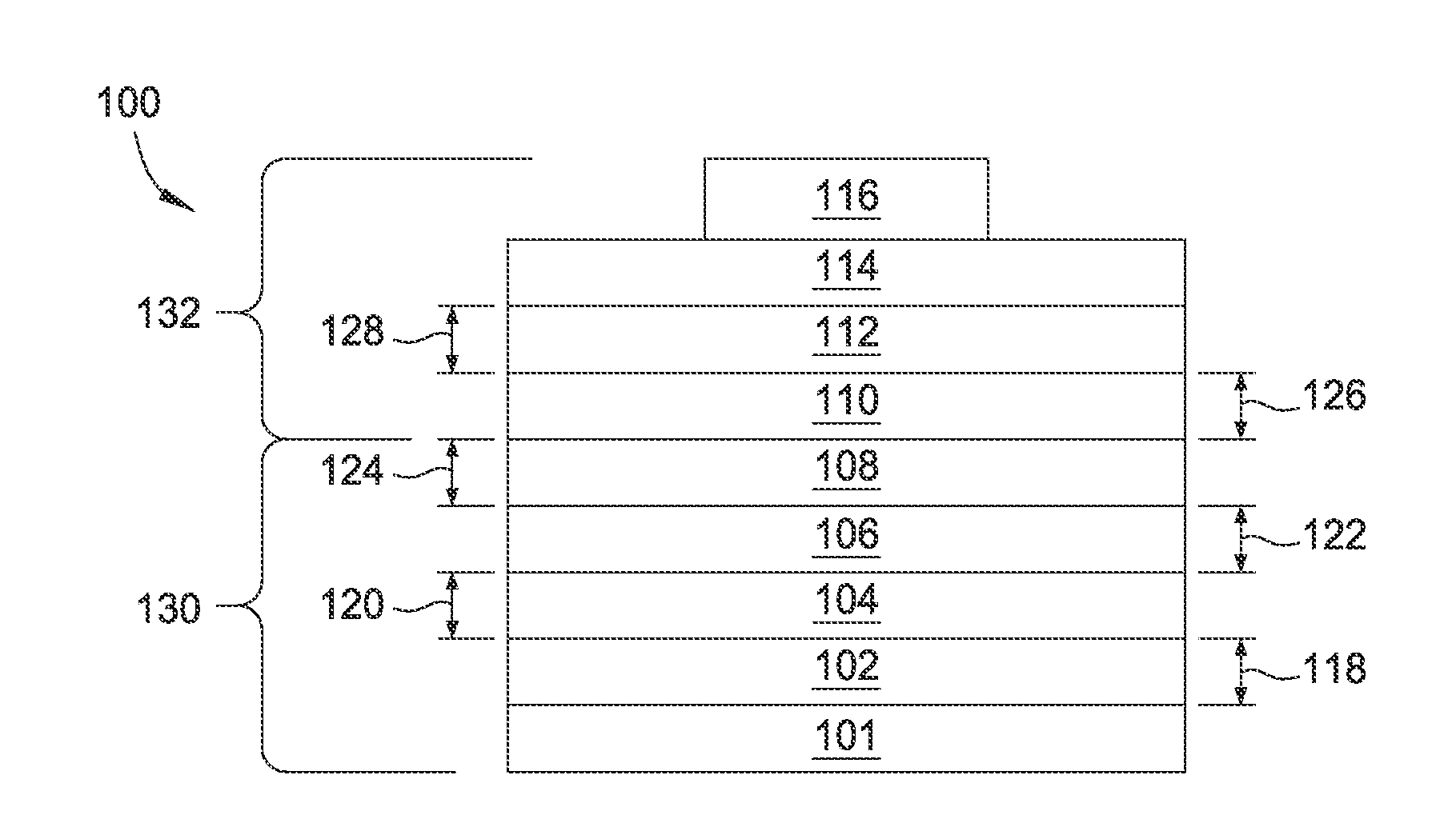
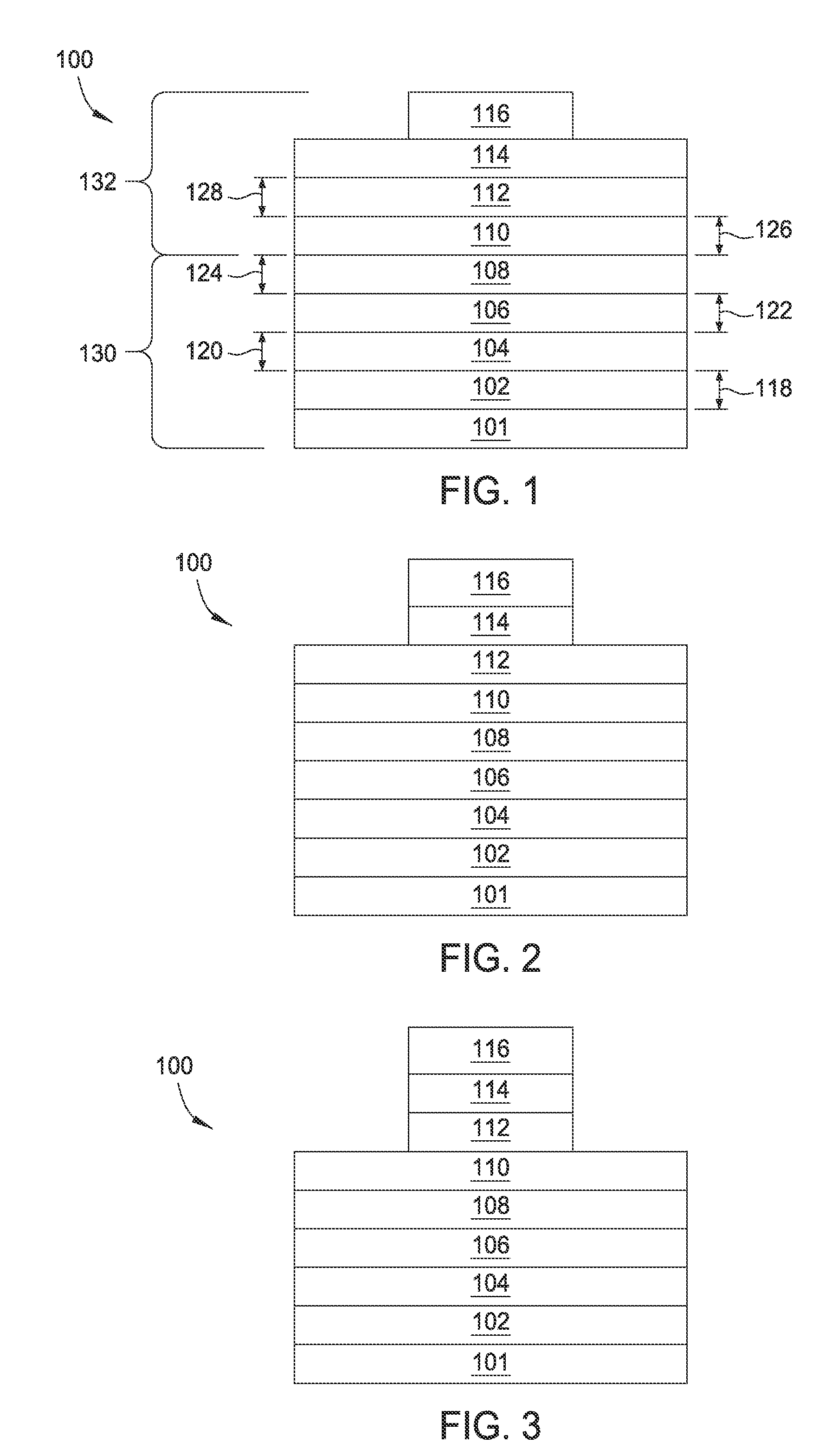
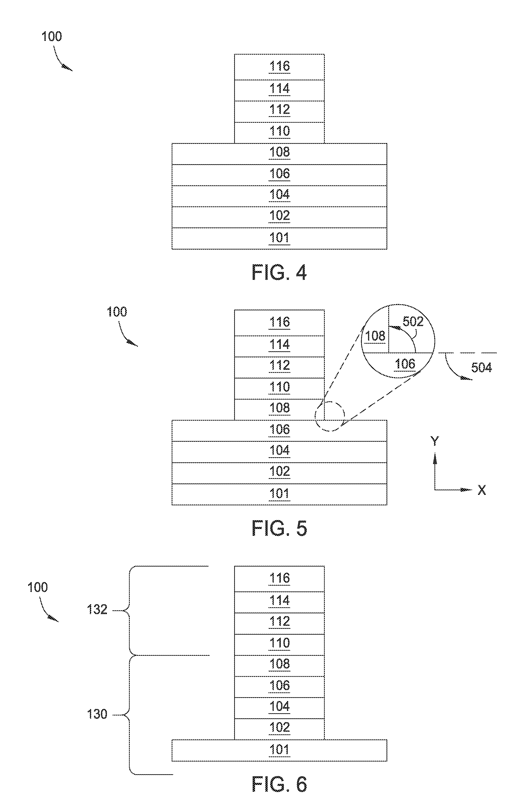
[0018]Device structures and methods for fabricating device structures are provided herein. Magneto-resistive random access memory (MRAM) devices described herein may include a film stack comprising a magnetic tunneling junction layer, a dielectric capping layer, an etch stop layer, a conductive hard mask layer, a dielectric hard mask layer, a spin on carbon layer, and an anti-reflective coating layer. The film stack may be etched by one or more selected chemistries to achieve improved film stack sidewall verticality. Memory cells having increasingly uniform and reduced critical dimensions may be fabricated utilizing the methods and devices described herein.

[0019]The various layers of the film stack may be utilized as hard masks for patterning the stack. The materials of the hard masks and etching chemistries utilized to etch the film stack may provide for improved etch selectivity which results in an improved sidewall verticality profile of features and structures formed on the film...


PUM

PropertyMeasurementUnit
sidewall angleaaaaaaaaaa
poweraaaaaaaaaa
poweraaaaaaaaaa

Abstract

Device structures and methods for fabricating device structures are provided herein. Magnetic random access memory (MRAM) devices described herein may include a film stack comprising a magnetic tunneling junction layer, a dielectric capping layer, an etch stop layer, a conductive hard mask layer, a dielectric hard mask layer, a spin on carbon layer, and an anti-reflective coating layer. The film stack may be etched by one or more selected chemistries to achieve improved film stack sidewall verticality. Memory cells having increasingly uniform and reduced critical dimensions may be fabricated utilizing the methods and devices described herein.

Description

CROSS-REFERENCE TO RELATED APPLICATIONS[0001]This application claims benefit of U.S. Provisional Patent Application No. 62 / 168,756, filed May 30, 2015, the entirety of which is herein incorporated by reference.BACKGROUNDField[0002]Embodiments of the present disclosure generally relate to device structures and methods for forming device structures. More specifically, embodiments described herein relate to hard masks for patterning magnetic tunnel junctions (MTJs).Description of the Related Art[0003]Microelectronic devices are generally fabricated on a semiconductor substrate as integrated circuits. An example of such a device is a magnetic random access memory (MRAM). An MRAM device generally includes magnetic multilayer film stacks which are used as storage elements. The film stacks are typically a stack of different layers composed of various material, for example, permalloy (NiFe), cobalt iron (CoFe), tantalum (Ta), copper (Cu) and the like. The film stacks may also contain insula...

Claims


Application Information

Patent Timeline
Patent Type & Authority Applications(United States)
IPC IPC(8): H01L43/12H01L43/08H01L43/02
CPCH01L43/12H01L43/08H01L43/02H10N50/80H10N50/01H10N50/85H10N50/10
Inventor XUE, LINPAKALA, MAHENDRACHEN, HAOAHN, JAESOO
Owner APPLIED MATERIALS INC
Why Eureka
Try Eureka