Conductive Metallic and Semiconductor Ink Composition

a technology of conductive inks and compositions, applied in the direction of inks, metal/alloy conductors, conductors, etc., can solve the problems of inability to utilize, conductive inks may not be suitable for forming ohmic contacts, and the fabrication technique of forming ohmic contacts to a semiconductor substrate does not scale well for devices larger than a semiconductor wafer, so as to achieve stable conductor

Inactive Publication Date: 2014-02-20
NTHDEGREE TECH WORLDWIDE
View PDF14 Cites 27 Cited by
  • Summary
  • Abstract
  • Description
  • Claims
  • Application Information

AI Technical Summary

Benefits of technology

[0005]Representative embodiments provide a “metallic and semiconductor nanoparticle ink” and a “metallic nanoparticle ink”, namely, a liquid or gel suspension of metallic nanoparticles or metallic nanoparticles with semiconductor nanoparticles (and also metallic microparticles and / or semiconductor microparticles in selected embodiments), which is capable of being printed, such as through screen printing or flexographic printing, for example and without limitation, to produce a substantially stable conductor when annealed.

Problems solved by technology

While such inks produce conductors (when cured) which are substantially conductive and have a comparatively low electrical impedance (or resistance), when such inks are to be utilized for bonding to other, second conductors, the curing temperatures for such conductive inks may exceed the melting temperature of such second conductors and cannot be utilized.
In addition, such conductive inks may not be suitable for forming ohmic contacts directly with a semiconductor substrate such as silicon.
Such fabrication techniques for forming ohmic contacts to a semiconductor substrate do not scale well for devices larger than a semiconductor wafer.
In addition, depending upon the processing techniques, some of the semiconductor substrate may be lost or deformed, which may be significant when trying to preserve a specific shape, such as substantially spherical, of the semiconductor substrate.

Method used


Image

  • Conductive Metallic and Semiconductor Ink Composition
  • Conductive Metallic and Semiconductor Ink Composition
  • Conductive Metallic and Semiconductor Ink Composition

Examples


Embodiment Construction

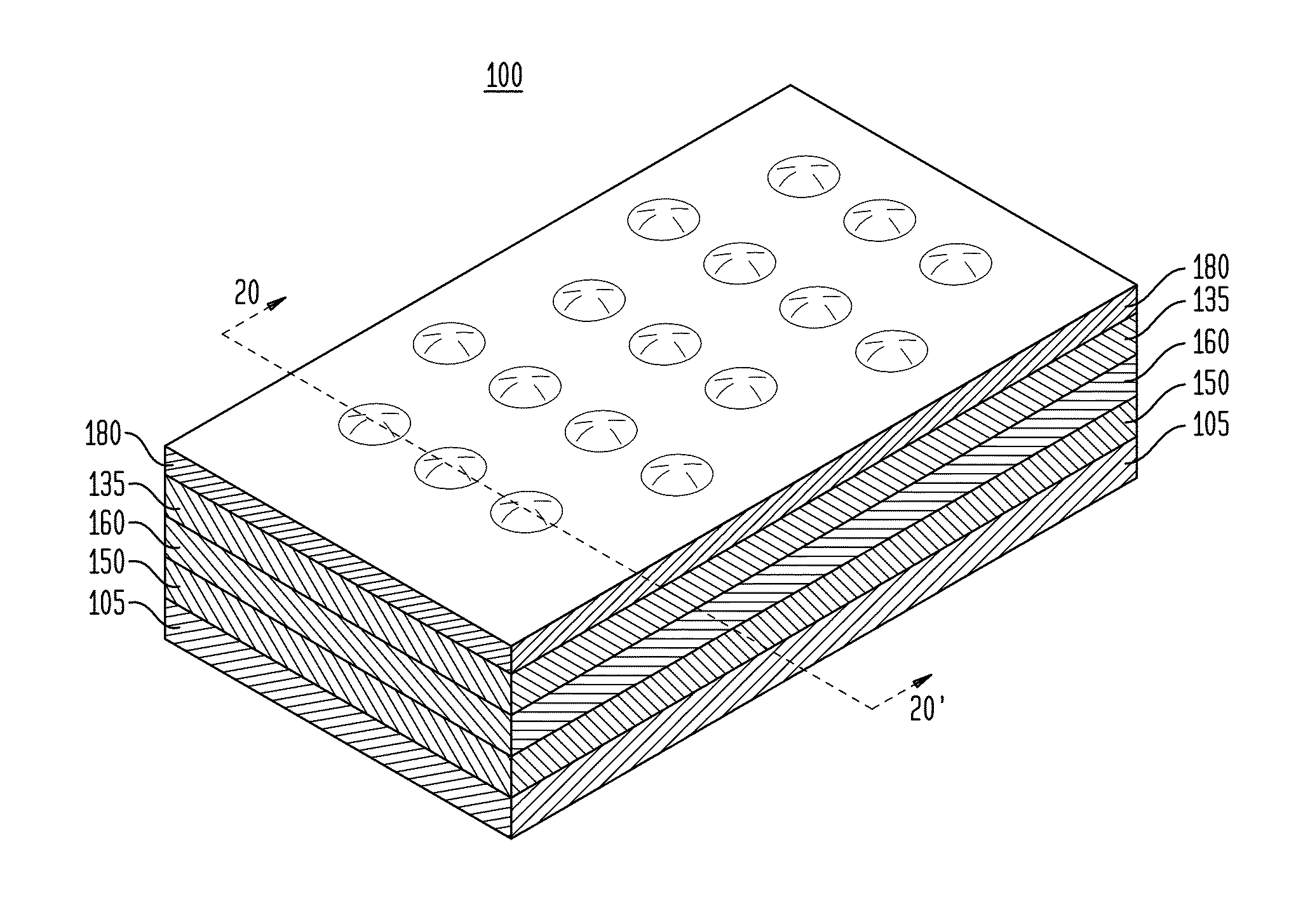
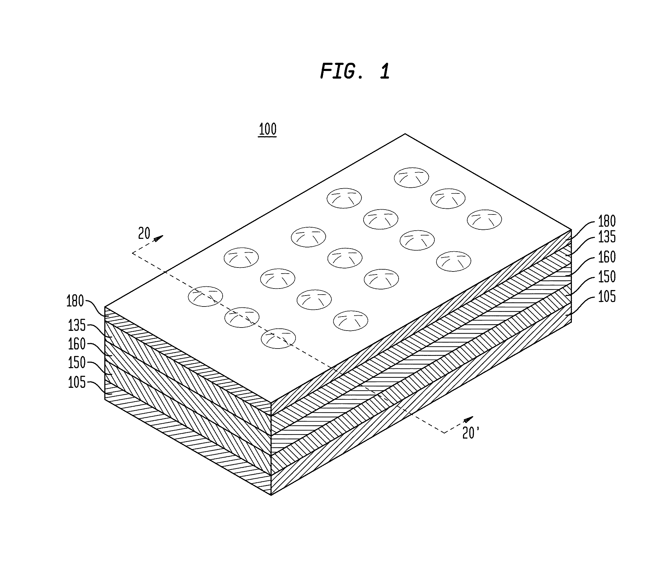
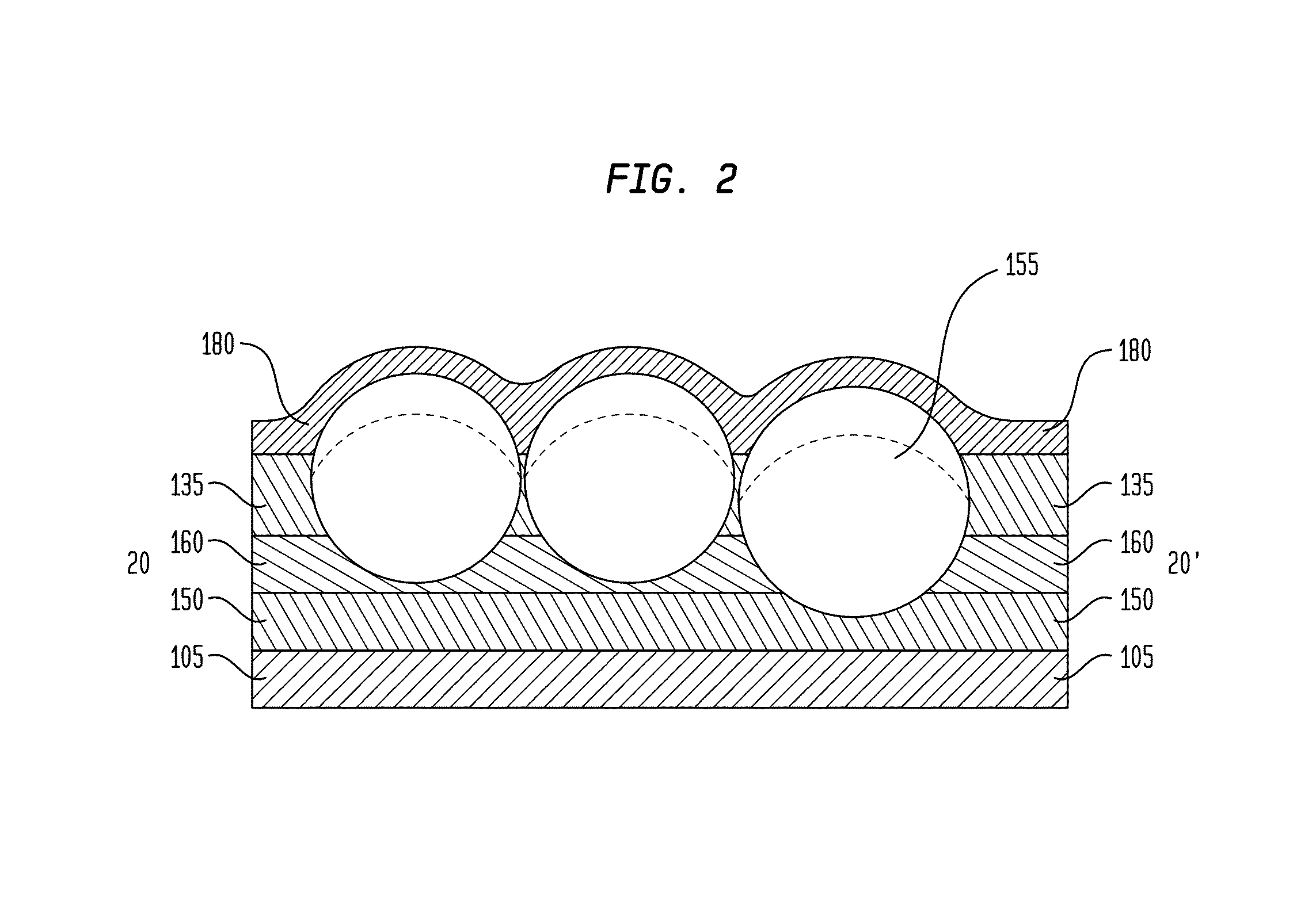
[0046]While the present invention is susceptible of embodiment in many different forms, there are shown in the drawings and will be described herein in detail specific exemplary embodiments thereof, with the understanding that the present disclosure is to be considered as an exemplification of the principles of the invention and is not intended to limit the invention to the specific embodiments illustrated. In this respect, before explaining at least one embodiment consistent with the present invention in detail, it is to be understood that the invention is not limited in its application to the details of construction and to the arrangements of components set forth above and below, illustrated in the drawings, or as described in the examples. Methods and apparatuses consistent with the present invention are capable of other embodiments and of being practiced and carried out in various ways. Also, it is to be understood that the phraseology and terminology employed herein, as well as...


PUM

PropertyMeasurementUnit
sizeaaaaaaaaaa
sizesaaaaaaaaaa
sizesaaaaaaaaaa

Abstract

A representative printable composition comprises a liquid or gel suspension of a plurality of metallic particles; a plurality of semiconductor particles; and a first solvent. The pluralities of particles may also be comprised of an alloy of a metal and a semiconductor. The composition may further comprise a second solvent different from the first solvent. In a representative embodiment, the first solvent comprises a polyol or mixtures thereof, such as glycerin, and the second solvent comprises a carboxylic or dicarboxylic acid or mixtures thereof, such as glutaric acid. In various embodiments, the metallic particles and the semiconductor particles are nanoparticles between about 5 nm to about 1.5 microns in any dimension. A representative metallic and semiconductor particle ink can be printed and annealed to produce a conductor.

Description

FIELD OF THE INVENTION[0001]The present invention in general is related to compositions for conductive inks and polymers utilized to produce a conductor, deposition methods and resulting apparatuses.BACKGROUND OF THE INVENTION[0002]Many conductive inks include a particulate metal, such as silver or aluminum, in a binder or binding medium. While such inks produce conductors (when cured) which are substantially conductive and have a comparatively low electrical impedance (or resistance), when such inks are to be utilized for bonding to other, second conductors, the curing temperatures for such conductive inks may exceed the melting temperature of such second conductors and cannot be utilized. In addition, such conductive inks may not be suitable for forming ohmic contacts directly with a semiconductor substrate such as silicon. Instead, such conductive inks are typically utilized to form circuit board traces for coupling to metal contacts created as part of integrated circuit packagin...

Claims


Application Information

Patent Timeline
Patent Type & Authority Applications(United States)
IPC IPC(8): C09D11/00H01L21/288
CPCH01L21/288C09D11/52
Inventor LOCKETT, VERA NICHOLAEVNALOWENTHAL, MARK DAVIDSHOTTON, NEIL O.RAY, WILLIAM JOHNSTONEYOUNGBULL, TRICIAKAMINS, THEODORE I.
Owner NTHDEGREE TECH WORLDWIDE
Why Eureka
Try Eureka