Semiconductor device and method of manufacturing the same

a semiconductor and semiconductor technology, applied in semiconductor devices, instruments, electrical devices, etc., can solve the problems of limited degree of integration of 3d non-volatile memory devices, physical limits of increasing the degree of integration of substrates, and the inability to manufacture memory cells in two-dimensional memory devices, etc., to achieve the effect of increasing the degree of integration

Active Publication Date: 2014-03-06
SK HYNIX INC
View PDF10 Cites 111 Cited by
  • Summary
  • Abstract
  • Description
  • Claims
  • Application Information

AI Technical Summary

Benefits of technology

[0007]An embodiment of the present invention relates to a semiconductor devic

Problems solved by technology

Two-dimensional memory devices in which memory cells are fabricated in a single layer over a substrate have reached physical limits in increasing their degree of integration.
In

Method used


Image

  • Semiconductor device and method of manufacturing the same
  • Semiconductor device and method of manufacturing the same
  • Semiconductor device and method of manufacturing the same

Examples


first embodiment

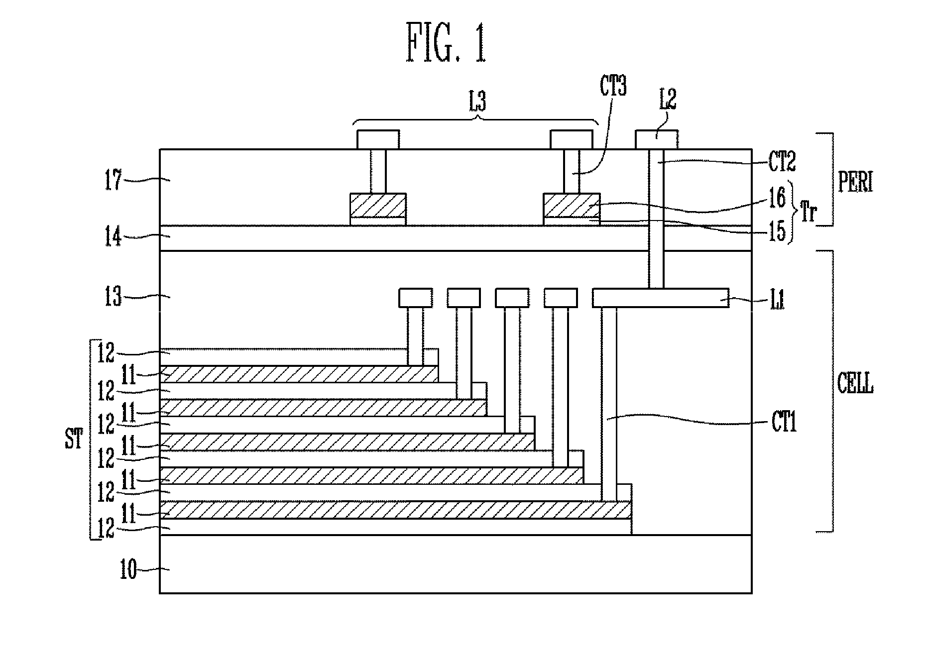
[0024]FIG. 1 is a cross-sectional view of a structure of a semiconductor device according the present invention.

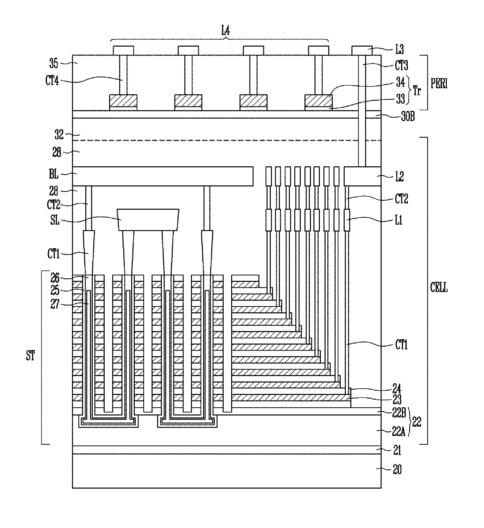
[0025]As illustrated in FIG. 1, the semiconductor device according to the first embodiment includes a first substrate 10, a second substrate 14 located over the first substrate 10, and at least one line, e.g., a second line L2. A cell region CELL in which memory cells are stacked is defined on the first substrate 10. A peripheral region PERI is defined on the second substrate 14. The second line L2 is located in the peripheral region PERI. The second line L2 passes through the second substrate 14 and is coupled to the cell region CELL. As can be seen, the first substrate 10 and the second substrate 14 are non-contiguous and are positioned along different planes.

[0026]The cell region CELL refers to a region where the memory cells are formed. The peripheral region PERI refers to a region where transistors configured to provide access to the memory cells are formed.

[0027]In a...

second embodiment

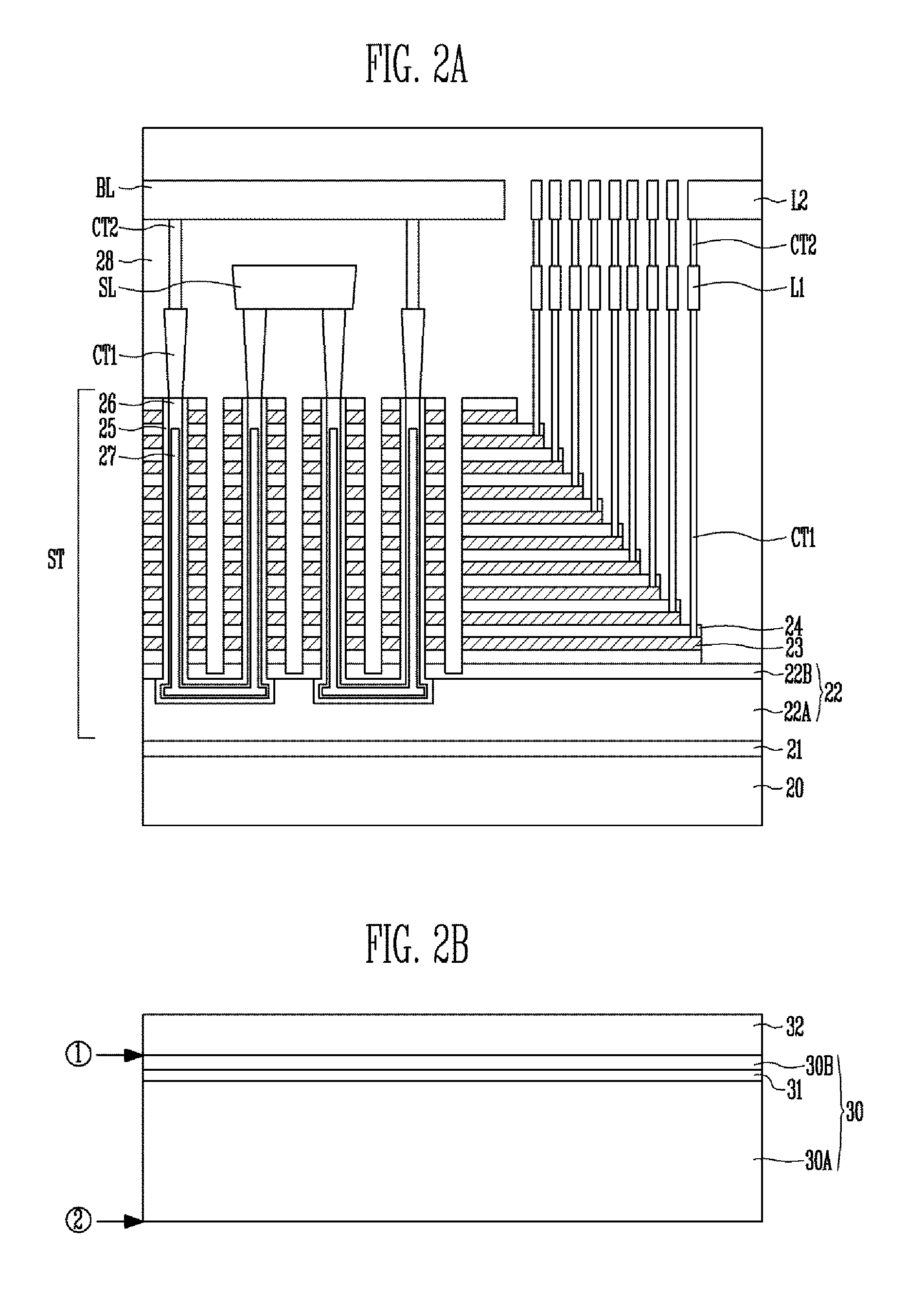
[0053]As illustrated in FIG. 3, the semiconductor device includes a first substrate 40, a second substrate 47 and at least one line, e.g., a second line L2. The first substrate 40 includes a cell region CELL formed along a first surface ① and a peripheral region PERI formed along a second surface ② thereof. The second substrate 47 is formed under the cell region CELL, and the second line L2 is formed in the peripheral region PERI. The second line L2 extends through the first substrate 40 and is coupled to the cell region CELL. The first surface ① may be a rear surface of the first substrate 40, and the second surface ② may be a top surface of the first substrate 40.

[0054]In addition, the semiconductor device may further include a stacked structure ST, a first interlayer insulating layer 43, a second interlayer insulating layer 44 and one or more transistors Tr. The stacked structure ST includes one or more first material layers 41 and one or more second material layers that are for...


PUM


Abstract

A semiconductor memory device includes a first substrate on which a cell region is defined. In the cell region, memory cells are stacked. A second substrate is located above the first substrate, and a peripheral region is defined on the second substrate. One or more conductive lines are located in the peripheral region. The one or more lines extend through the second substrate and couple to the cell region.

Description

CROSS-REFERENCE TO RELATED APPLICATION[0001]The present application claims priority to Korean patent application number 10-2012-0096464 filed on Aug. 31, 2012, in the Korean Intellectual Property Office, the entire disclosure of which is incorporated by reference herein.BACKGROUND[0002]1. Technical Field[0003]Various embodiments relate generally to a semiconductor device and a method of manufacturing the same and, more particularly, to a semiconductor device including a stacked body and a method of manufacturing the same.[0004]2. Related Art[0005]A non-volatile memory device retains data stored therein even when not powered. Two-dimensional memory devices in which memory cells are fabricated in a single layer over a substrate have reached physical limits in increasing their degree of integration. Accordingly, three-dimensional (3D) non-volatile memory devices in which memory cells are stacked in a vertical direction over a substrate have been proposed.[0006]A 3D non-volatile memory ...

Claims


Application Information

Patent Timeline
IPC IPC(8): H01L27/105
CPCH01L27/1052G11C5/025H01L27/0688G11C5/063H10B41/42H10B41/27H10B43/50H10B43/40H10B43/27H01L21/2007H01L21/76205H10B99/00H10B41/40H10B41/41
Inventor KWON, OH CHULLEE, KI HONGPYI, SEUNG HO
Owner SK HYNIX INC
Why Eureka
Try Eureka