Integrated circuits with selective gate electrode recess

a gate electrode recess and integrated circuit technology, applied in the field of integrated circuits, can solve the problems of high-k film, parasitic transistor gate electrode capacitance is an ever more significant limiter of device performance, and high-k gate dielectrics may also adversely affect parasitic capacitan

Active Publication Date: 2014-03-13
INTEL CORP
View PDF5 Cites 140 Cited by
  • Summary
  • Abstract
  • Description
  • Claims
  • Application Information

AI Technical Summary

Problems solved by technology

In modern complementary metal-oxide-semiconductor (CMOS) technology, parasitic transistor gate electrode capacitance is an ever more significant limiter of device performance.
The introduction of high-k gate dielectrics ...

Method used


Image

  • Integrated circuits with selective gate electrode recess
  • Integrated circuits with selective gate electrode recess
  • Integrated circuits with selective gate electrode recess

Examples


Embodiment Construction

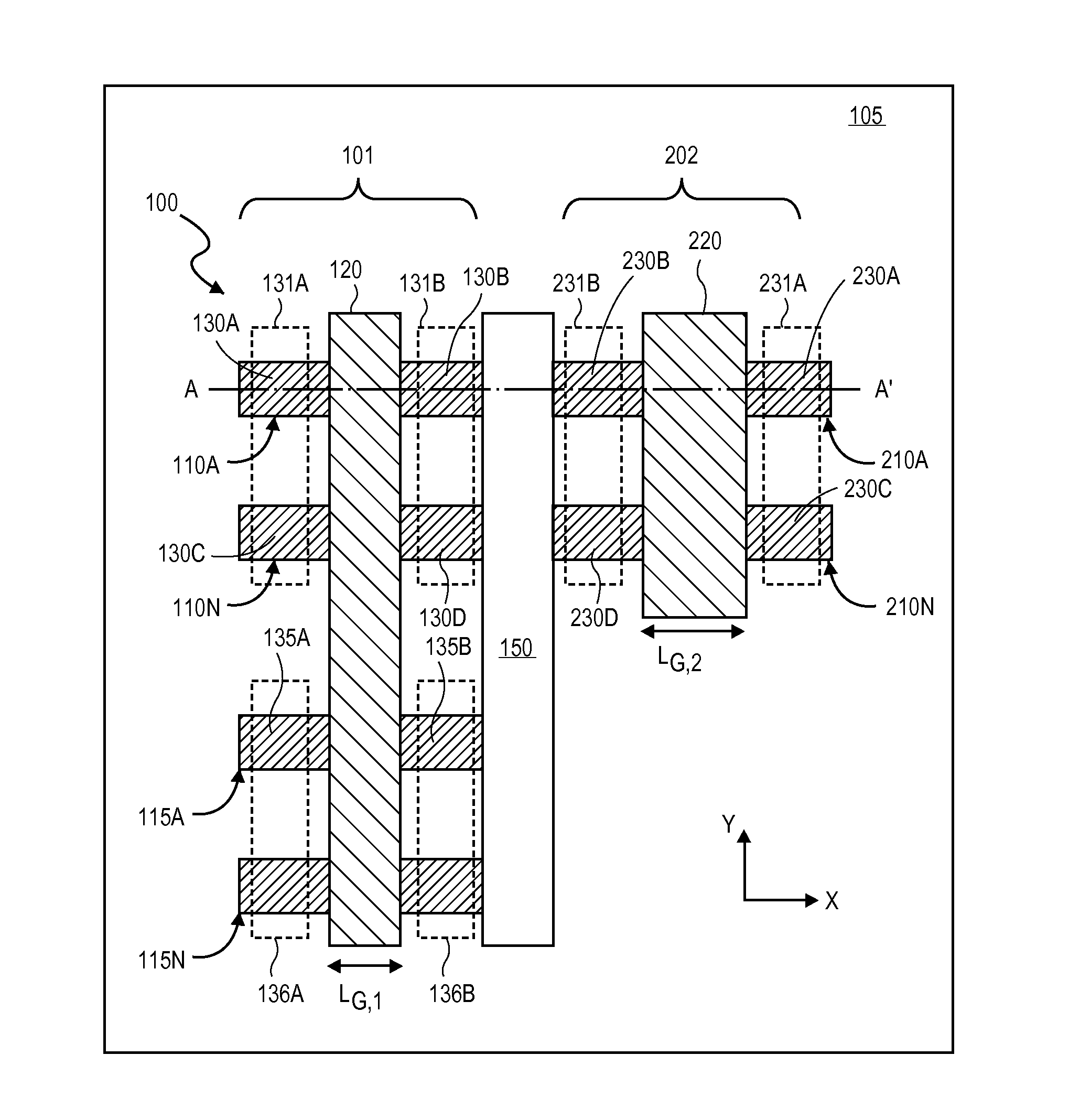
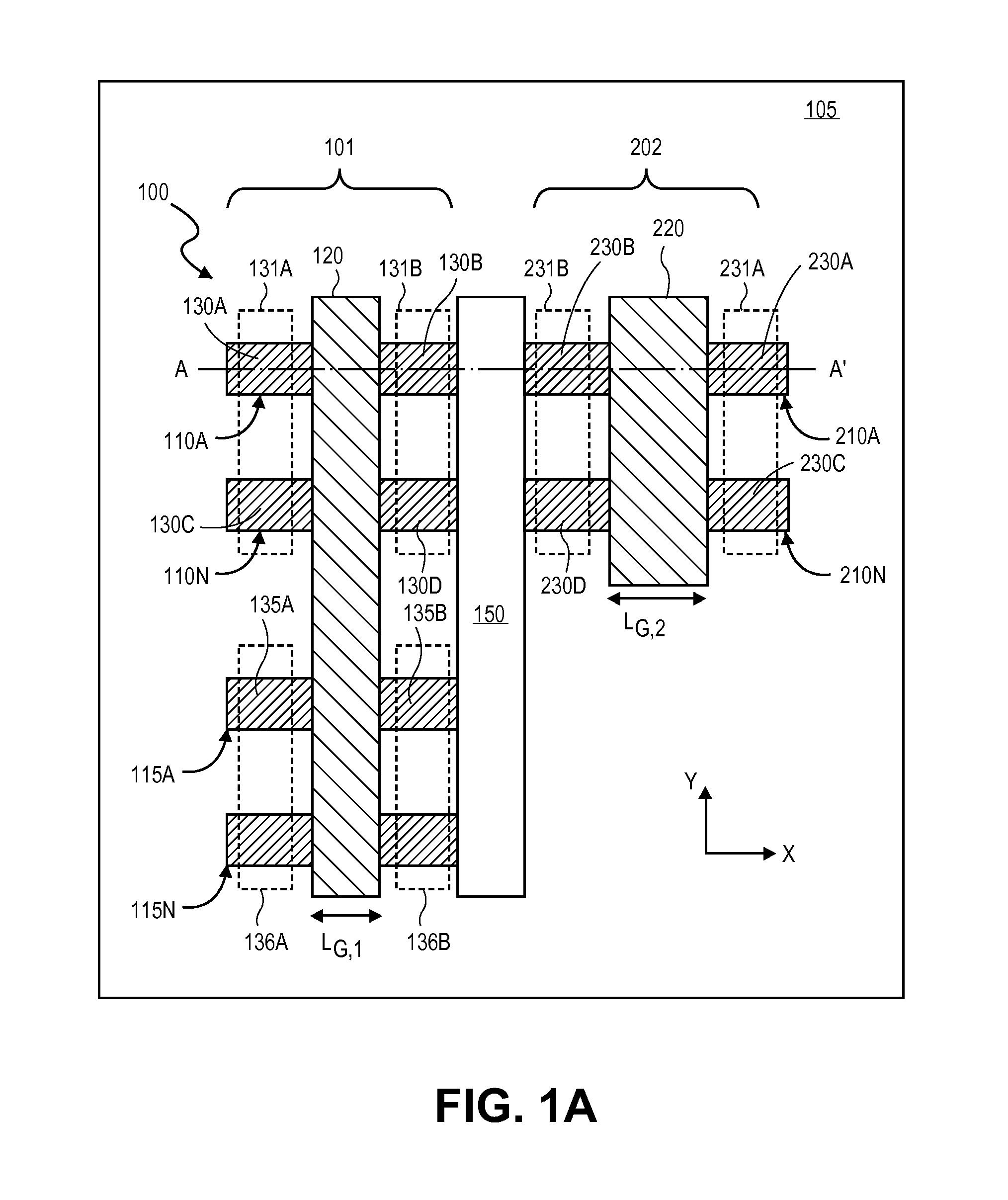
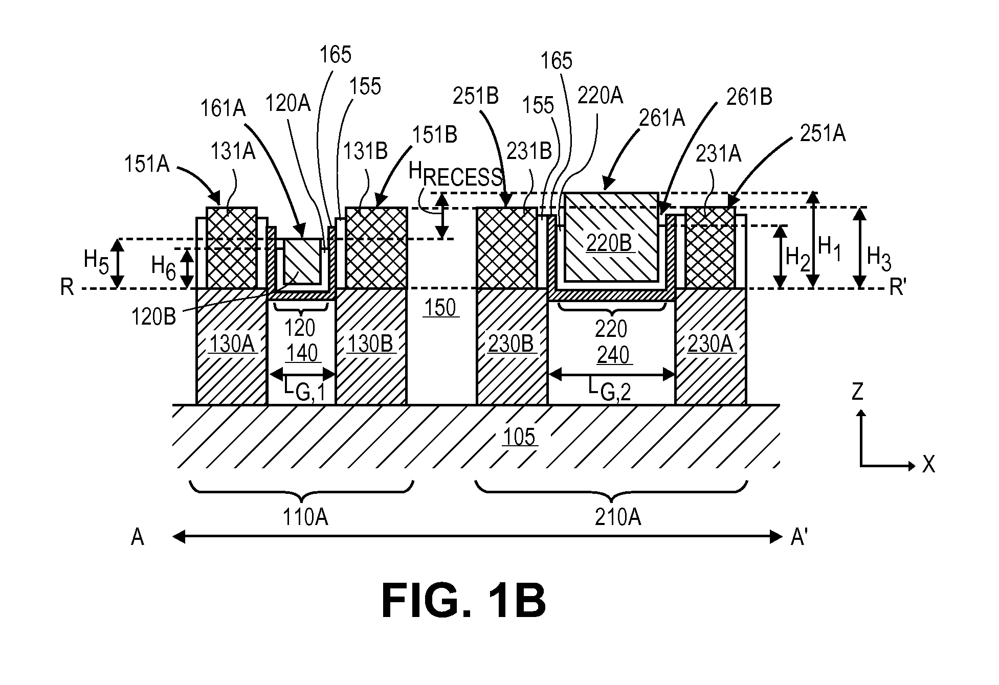
[0012]In the following description, numerous details are set forth, however, it will be apparent to one skilled in the art, that the present invention may be practiced without these specific details. In some instances, well-known methods and devices are shown in block diagram form, rather than in detail, to avoid obscuring the present invention. Reference throughout this specification to “an embodiment” or “in one embodiment” means that a particular feature, structure, function, or characteristic described in connection with the embodiment is included in at least one embodiment of the invention. Thus, the appearances of the phrase “in an embodiment” in various places throughout this specification are not necessarily referring to the same embodiment of the invention. Furthermore, the particular features, structures, functions, or characteristics may be combined in any suitable manner in one or more embodiments. For example, a first embodiment may be combined with a second embodiment ...


PUM


Abstract

Integrated circuits including MOSFETs with selectively recessed gate electrodes. Transistors having recessed gate electrodes with reduced capacitive coupling area to adjacent source and drain contact metallization are provided alongside transistors with gate electrodes that are non-recessed and have greater z-height. In embodiments, analog circuits employ transistors with gate electrodes of a given z-height while logic gates employ transistors with recessed gate electrodes of lesser z-height. In embodiments, subsets of substantially planar gate electrodes are selectively etched back to differentiate a height of the gate electrode based on a given transistor's application within a circuit.

Description

TECHNICAL FIELD[0001]Embodiments of the invention generally relate to integrated circuits (ICs), and more particularly relate to transistor gate electrode structures where some gate electrodes are recessed relative to other gate electrodes.BACKGROUND[0002]In modern complementary metal-oxide-semiconductor (CMOS) technology, parasitic transistor gate electrode capacitance is an ever more significant limiter of device performance. With device scaling, reductions in feature pitch continue to reduce distances between electrical nodes of a physical transistor. The introduction of high-k gate dielectrics may also adversely impact parasitic capacitances, for example where fabrication of the high-k gate dielectrics results in high-k films in regions other than at the interface between a transistor channel and the gate electrode. Furthermore, in addition to scaling and new materials introductions, structure geometries are now changing dramatically as the microelectronics industry now transiti...

Claims


Application Information

Patent Timeline
IPC IPC(8): H01L27/088H01L29/66
CPCH01L27/0886H01L29/66477H01L27/088H01L21/823821H01L27/0924H01L21/823456H01L21/82385H10B10/12H01L21/28008H01L21/823431H01L29/495
Inventor MUKHERJEE, SRIJITWIEGAND, CHRISTOPHER J.WEEKS, IVLER .LIU, MARK Y.HATTENDORF, MICHAEL L.
Owner INTEL CORP
Why Eureka
Try Eureka