Substrate integrated waveguide coupler

a technology of integrated waveguides and substrates, applied in the direction of waveguides, sustainable waste treatment, manufacturing tools, etc., can solve the problems of transmission loss and induce transmission loss, and achieve the effect of reducing transmission loss and reducing signal leakag

Inactive Publication Date: 2014-03-20
ELECTRONICS & TELECOMM RES INST
View PDF2 Cites 9 Cited by
  • Summary
  • Abstract
  • Description
  • Claims
  • Application Information

AI Technical Summary

Benefits of technology

[0020]According to exemplary embodiments of the present invention, it is possible to form pipeline type via holes to be disposed mutually parallel to each other at both sides of a substrate integrat

Problems solved by technology

However, this type of cylindrical via hole structure induces the occurrence of transmissi

Method used


Image

  • Substrate integrated waveguide coupler
  • Substrate integrated waveguide coupler
  • Substrate integrated waveguide coupler

Examples


Embodiment Construction

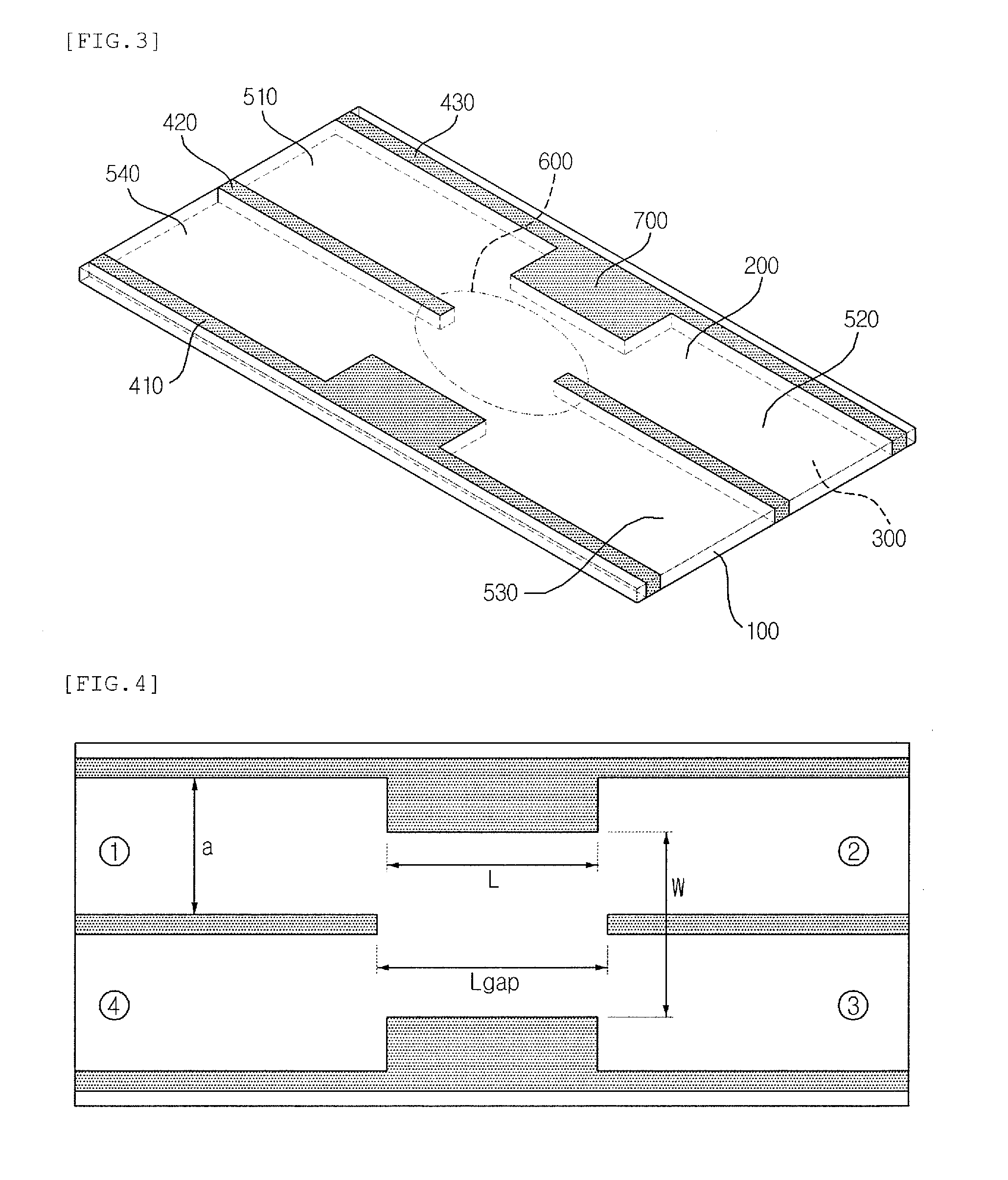
[0033]Hereinafter, a substrate integrated waveguide coupler according to exemplary embodiments of the present invention will be described in detail with reference to the accompanying drawings, FIGS. 2 to 8. The detailed description will focus on elements required for the understanding of the operation and effects according to the present invention.

[0034]Particularly, the present invention presents a novel structure having pipeline type via holes formed to be disposed mutually parallel to each other at both sides of the substrate integrated waveguide coupler, and having a preset section of the pipeline type via holes formed with at least one step.

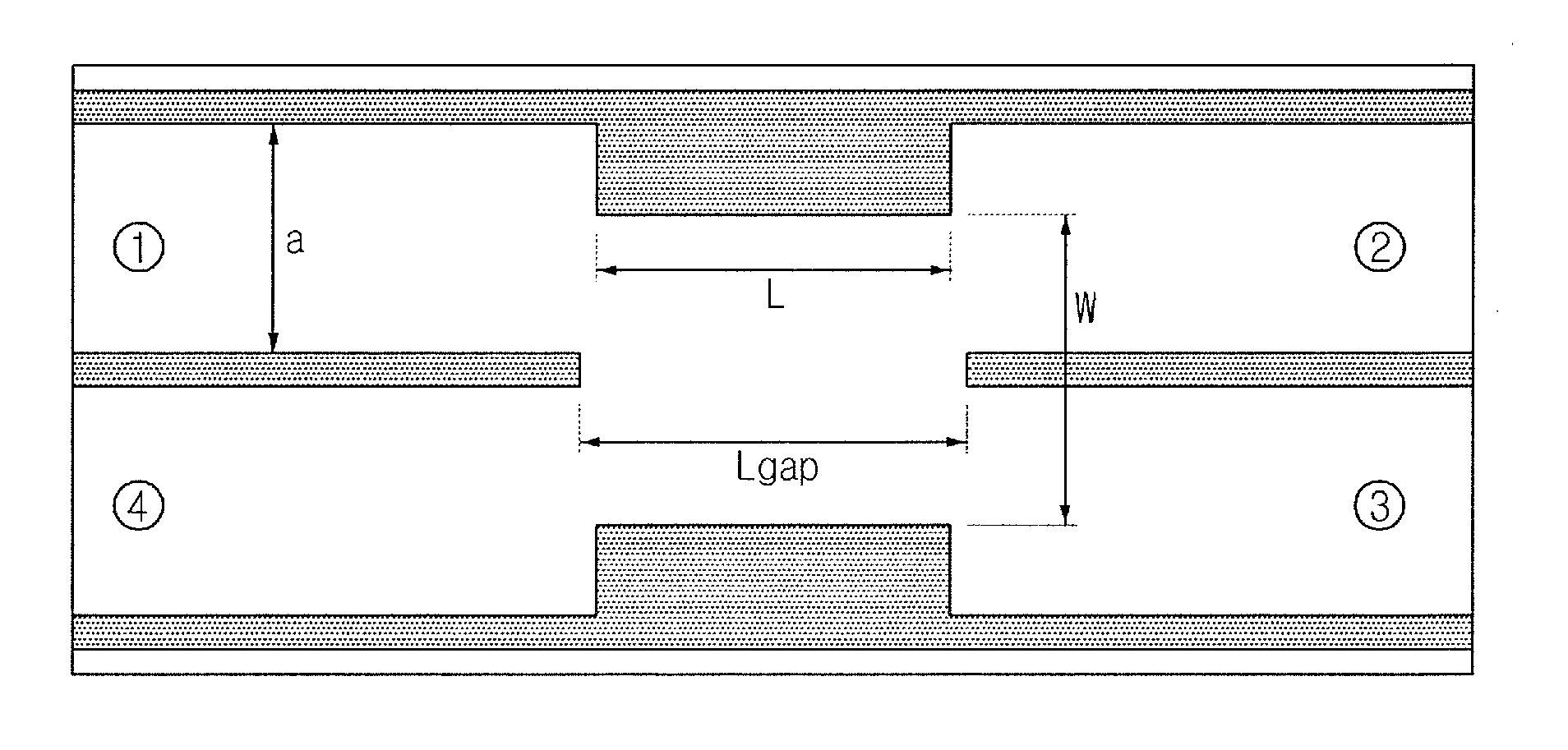
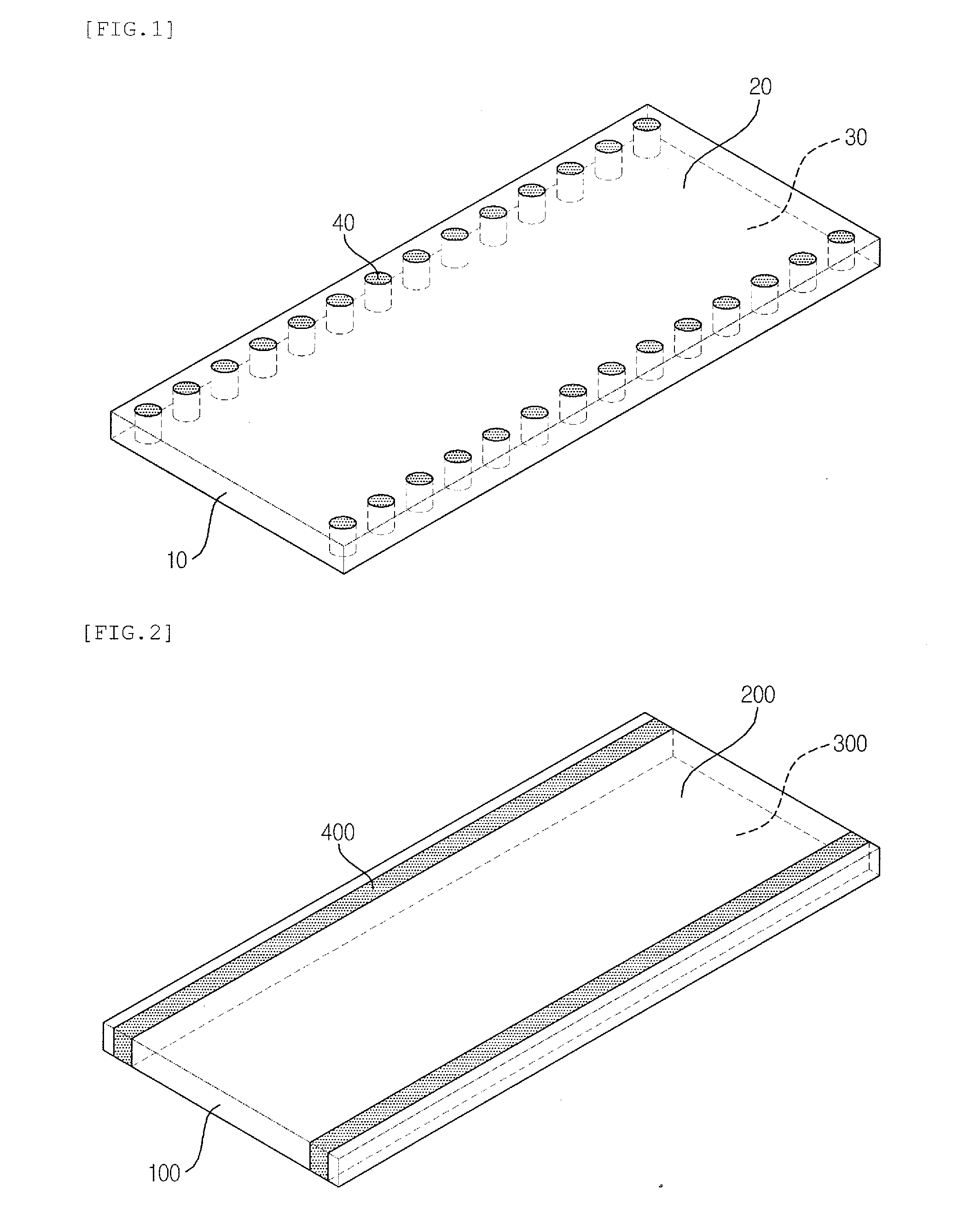
[0035]FIG. 2 is a diagram illustrating the structure of a substrate integrated waveguide according to an exemplary embodiment of the present invention.

[0036]Referring to FIG. 2, a substrate integrated waveguide according to the present invention may be configured to include a substrate 100, an upper conducting plate 200, a lower conducting p...


PUM

PropertyMeasurementUnit
Thicknessaaaaaaaaaa
Lengthaaaaaaaaaa
Sizeaaaaaaaaaa

Abstract

Disclosed is a substrate integrated waveguide coupler. The substrate integrated waveguide coupler according to the present invention includes: a substrate; an upper conducting plate applied to an upper portion of the substrate; a lower conducting plate applied to a lower portion of the substrate; two peripheral via holes disposed parallel to each other on both sides of the substrate, respectively, and being of a pipeline type electrically connecting the upper conducting plate and the lower conducting plate to each other; and an inner via hole disposed between the two peripheral via holes, and having a center thereof separated by a preset distance and forming a short slot functioning to couple input signals.

Description

CROSS-REFERENCE TO RELATED APPLICATIONS[0001]This application claims priority to and the benefit of Korean Patent Application No. 10-2012-0103170 filed in the Korean Intellectual Property Office on Sep. 18, 2012, the entire contents of which are incorporated herein by reference.TECHNICAL FIELD[0002]The present invention relates to a substrate integrated waveguide coupler, and particularly, to a substrate integrated waveguide coupler having pipeline type via holes formed to be disposed mutually parallel to each other at both sides of the substrate integrated waveguide coupler, and having a preset section of the pipeline type via holes formed with at least one step.BACKGROUND ART[0003]A substrate integrated waveguide (SIW) is a structure in which the top surface and the bottom surface of a dielectric semiconductor are applied as a conductor, and via holes that electrically connect the conductors of both the upper and lower surfaces are disposed at regular intervals along the vertical ...

Claims


Application Information

Patent Timeline
IPC IPC(8): H01P5/02
CPCH03H7/38H01P3/006C04B26/18C04B2111/56Y02W30/91C04B14/06C04B18/141C04B20/0096C04B26/04C04B14/04C04B18/14B28B21/30
Inventor LEE, HONG YEOLUHM, MAN SEOKYUN, SO HYEUNKWAK, CHANG SOOCHOI, JANG SUPYOM, IN BOK
Owner ELECTRONICS & TELECOMM RES INST
Why Eureka
Try Eureka