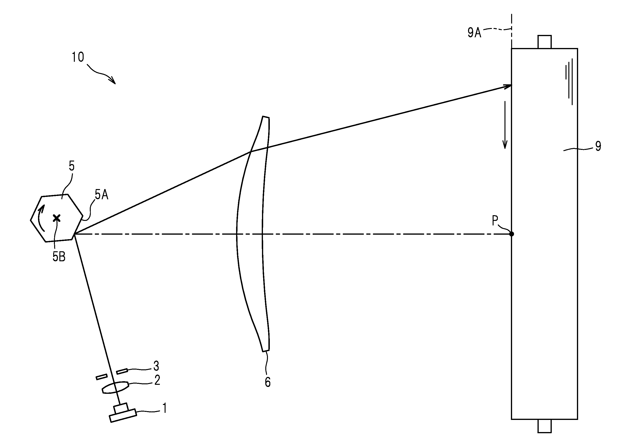
Scanning optical apparatus
- Summary
- Abstract
- Description
- Claims
- Application Information
AI Technical Summary
Benefits of technology
Problems solved by technology
Method used
Image

Examples
example 1
[0062]Example 1 illustrates a single-lens implementation of the illumination optical system in which an ellipsoidal diffractive surface and an anamorphic refractive surface are provided. The optical system I1 was configured as specified below, and the main scanning direction power ratio φnM / φdM and the sub-scanning direction power ratio φnS / φdS were adjusted so as to reduce the image plane shift associated with temperature change in a range of −5° C. to 55° C., by varying parameters of: (1) coefficient Z of linear expansion of the holding member provided to retain a distance between the light source (semiconductor laser) and the illumination optical system (diffraction lens), (2) magnification ratio mM / mS of the entire optical system (including the diffraction lens and the f-theta lens), and (3) focal length fi of the diffraction lens. The range of each parameter is as follows:
[0063]Coefficient Z of linear expansion: 3.0×10⁻⁵ to 9.5×10⁻⁵
[0064]Focal length fi [mm]: 10 to 30 mm
[0065]...
example 2
[0084]Example 2 illustrates a combined-lens implementation of the illumination optical system as shown in FIG. 4, in which a collimating lens 11 having a rotation-symmetric diffractive surface and a cylindrical lens 12 having a diffractive power and a refractive power only in the sub-scanning direction are provided. In this implementation as well, it has been confirmed that the image plane shift associated with temperature change in a range of −5° C. to 55° C. can be restricted to the range not exceeding ±3 mm by adjusting the main scanning direction power ratio φnM / φdM and the sub-scanning direction power ratio φnS / φdS in the ranges as described above. The optical system I2 was configured as specified below.
[0085]Wavelength of semiconductor laser: 788 [nm]
[0086]Rate of change in wavelength of semiconductor laser: 0.25 [nm / ° C.]
[0087]Phase function of diffractive surface:
φ=∑m∑nCNxmynN=0.5[(m+n)2+m+3n]
[0088]CN (quadric term) of the fourth surface (rotation-symmetric diffractive surfa...
example 3
[0092]Example 3 illustrates a single-lens implementation of the illumination optical system as shown in FIGS. 5A and 5B, in which a rotation-symmetric diffractive surface 21A and an anamorphic refractive surface 21B having a linearly-patterned diffractive surface are provided. In this implementation as well, it has been confirmed that the image plane shift associated with temperature change in a range of −5° C. to 55° C. can be restricted to the range not exceeding ±3 mm by adjusting the main scanning direction power ratio φnM / φdM and the sub-scanning direction power ratio φnS / φdS in the ranges as described above. The optical system I3 was configured as specified below.
[0093]Wavelength of semiconductor laser: 788 [nm]
[0094]Rate of change in wavelength of semiconductor laser: 0.25 [nm / ° C.]
[0095]Phase function of diffractive surface:
φ=∑m∑nCNxmynN=0.5[(m+n)2+m+3n]
[0096]CN (quadric term) of the fourth surface (rotation-symmetric diffractive surface): −0.01181
[0097]CN (quadric term) in ...
PUM
 Abstract
Description
Claims
Application Information