System and method for manufacturing thick and thin film devices using a donee layer cleaved from a crystalline donor

a donee layer and donor technology, applied in the field of film-based device manufacturing, can solve the problems of reducing device performance, reducing device performance, and severely restricting the maximum temperature to which a substrate may be exposed by polymers/plastics

Inactive Publication Date: 2010-03-30
VERSATILIS
View PDF25 Cites 210 Cited by
  • Summary
  • Abstract
  • Description
  • Claims
  • Application Information

AI Technical Summary

Problems solved by technology

To address these needs, previous approaches attempted to realize these devices by developing new, novel and expensive technologies.
However, polymers / plastics severely limit the maximum temperature a substrate may be exposed to during manufacturing.
Metal foils, albeit immune from this temperature limit, suffer from a multitude of other problems that diminish device performance.
This tailoring of manufacturing process parameters to suit the choice of substrate selection rather than device performance has resulted in less than ideal devices.
Unfortunately, most in-production SMOI techniques are too exotic and therefore too expensive to service the overall market segments where SMOI technology would otherwise be embraced.

Method used


Image

  • System and method for manufacturing thick and thin film devices using a donee layer cleaved from a crystalline donor
  • System and method for manufacturing thick and thin film devices using a donee layer cleaved from a crystalline donor
  • System and method for manufacturing thick and thin film devices using a donee layer cleaved from a crystalline donor

Examples


Embodiment Construction

A. Device Structures

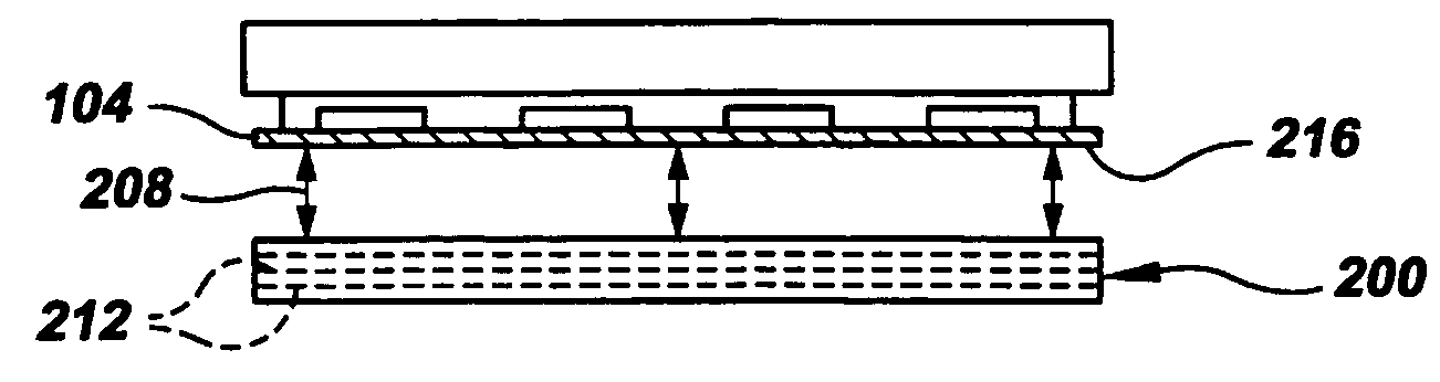
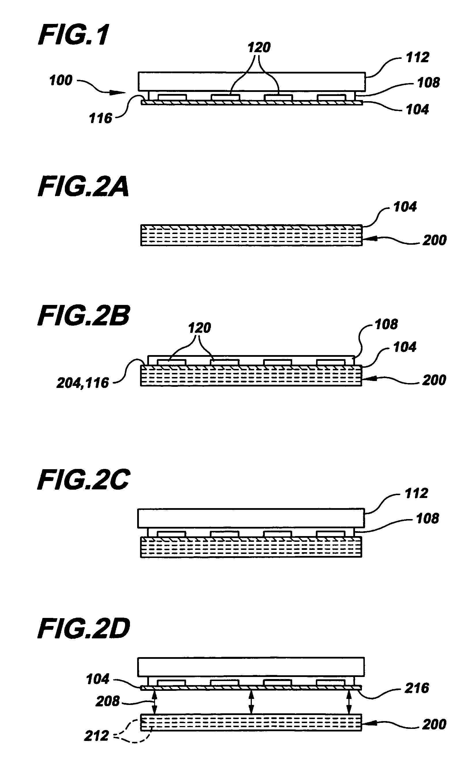
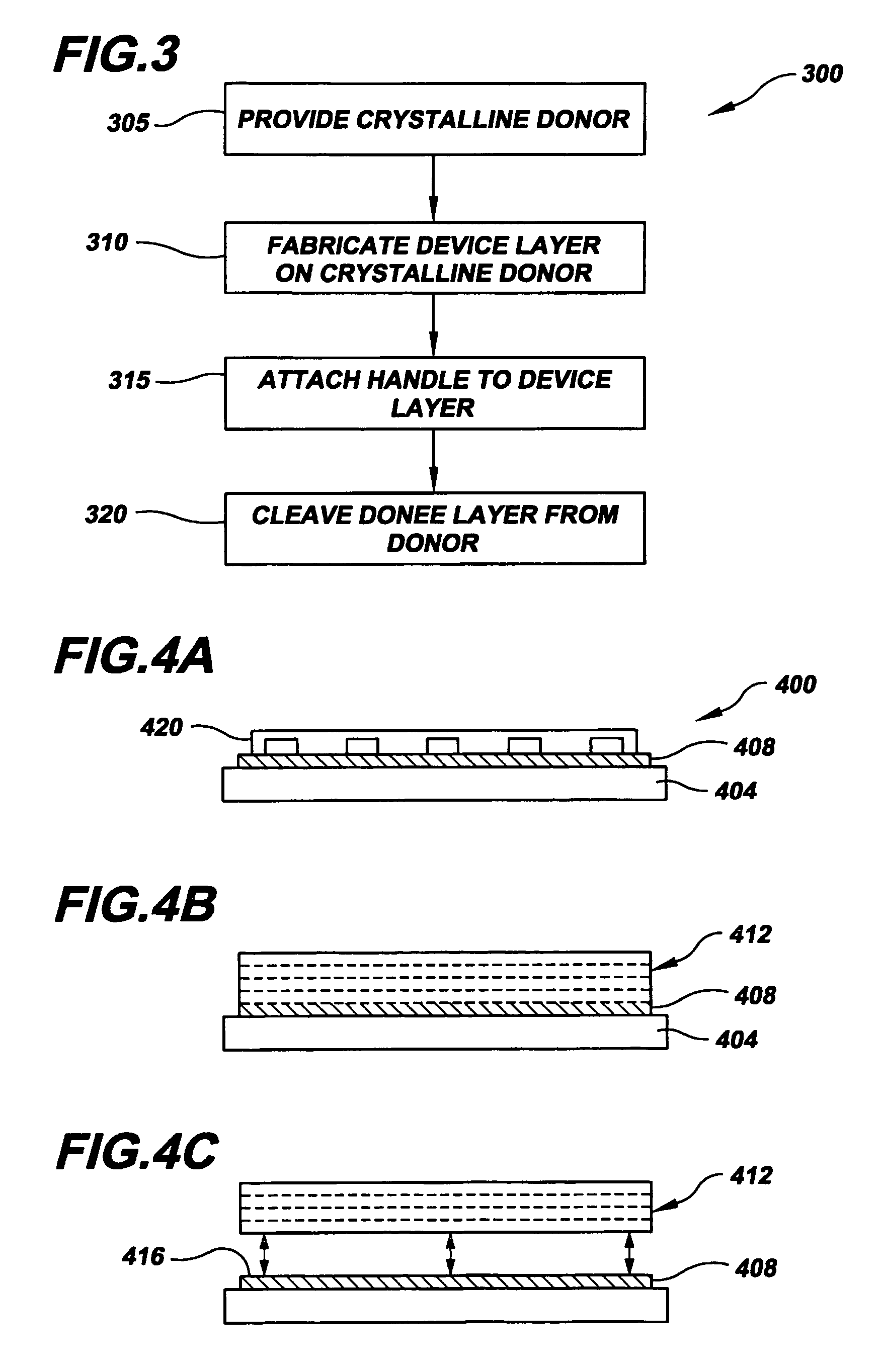
[0033]Referring now to the drawings, FIG. 1 illustrates a device structure 100 made in accordance with the present disclosure. At a high level, device structure 100 comprises a crystalline “donee” layer 104, a “device” layer 108 and a “handle”112. As discussed below in detail, donee layer 104 is a crystalline layer that has been cleaved from a crystalline “donor” (see donor 200 of FIG. 2A), which is essentially a mass of crystalline material that is able to provide at least one cleaved donee layer and, more typically, more than one donee layer. At its broadest, the present disclosure does not place any limitations on the donor other than it is crystalline in its atomic structure and that it may be cleaved so as to provide a crystalline surface, such as crystalline surface 116 suitable for use in creating a device structure, such as device structure 100. The donor may be virtually any naturally occurring mineral or synthetically produced crystal mass.

[0034]Two cla...


PUM

PropertyMeasurementUnit
thicknessaaaaaaaaaa
thicknessaaaaaaaaaa
thicknessaaaaaaaaaa

Abstract

Various embodiments of fabricated crystalline-based structures for the electronics, optoelectronics and optics industries are disclosed. Each of these structures is created in part by cleaving a donee layer from a crystalline donor, such as a micaceous / lamellar mass comprising a plurality of lamelliform sheets separable from each other along relatively weak cleavage planes. Once cleaved, one or more of these lamelliform sheets become the donee layer. The donee layer may be used for a variety of purposes, including a crystalline layer for supporting heteroepitaxial growth of one or more semiconductor layers thereon, an insulating layer, a barrier layer, a planarizing layer and a platform for creating useful structures, among others.

Description

RELATED APPLICATION DATA[0001]This application claims the benefit of priority of U.S. Provisional Patent Application Ser. No. 60 / 669,240, filed Apr. 8, 2005, and titled “Novel Method And Uses Of Transferred Thin Crystalline Films,” that is incorporated by reference herein in its entirety.FIELD OF THE INVENTION[0002]The present invention generally relates to the field of film-based device manufacturing. In particular, the present invention is directed to a system and method for manufacturing thick and thin film devices using a donee layer cleaved from a crystalline donor.BACKGROUND[0003]There is an ever-present need and desire to reduce the size, weight and cost of electronic devices we use without sacrificing performance. A wide range of devices from displays, electronics, sensors and optical components, to name just a few, would benefit from methodologies that would produce ruggedized, lightweight, portable, small form factor, less power hungry and lower cost devices. Furthermore, ...

Claims


Application Information

Patent Timeline
Patent Type & Authority Patents(United States)
IPC IPC(8): H01L21/30
CPCH01L21/187H01L21/6835H01L21/76251H01L27/1214H01L27/1266H01L29/78603Y10T428/24802H01L33/0079H01L2221/68359H01L2924/19041H01S5/0207Y10T156/12H01L29/78681H01L27/1218H01L33/0093H01L28/00
Inventor JAIN, AJAYKUMAR R.
Owner VERSATILIS
Why Eureka
Try Eureka