

Artificial medium, its manufacturing method, and antenna device
a technology of artificial medium and manufacturing method, which is applied in the direction of waveguides, paper/cardboard containers, line-transmission details, etc., can solve the problems of difficult downsizing (especially to thin) the artificial medium, increasing the production cost of the artificial medium, etc., and achieves the effect of manufacturing at a low cos
- Summary
- Abstract
- Description
- Claims
- Application Information
AI Technical Summary
Benefits of technology
Problems solved by technology
Method used
Image

Examples
first embodiment
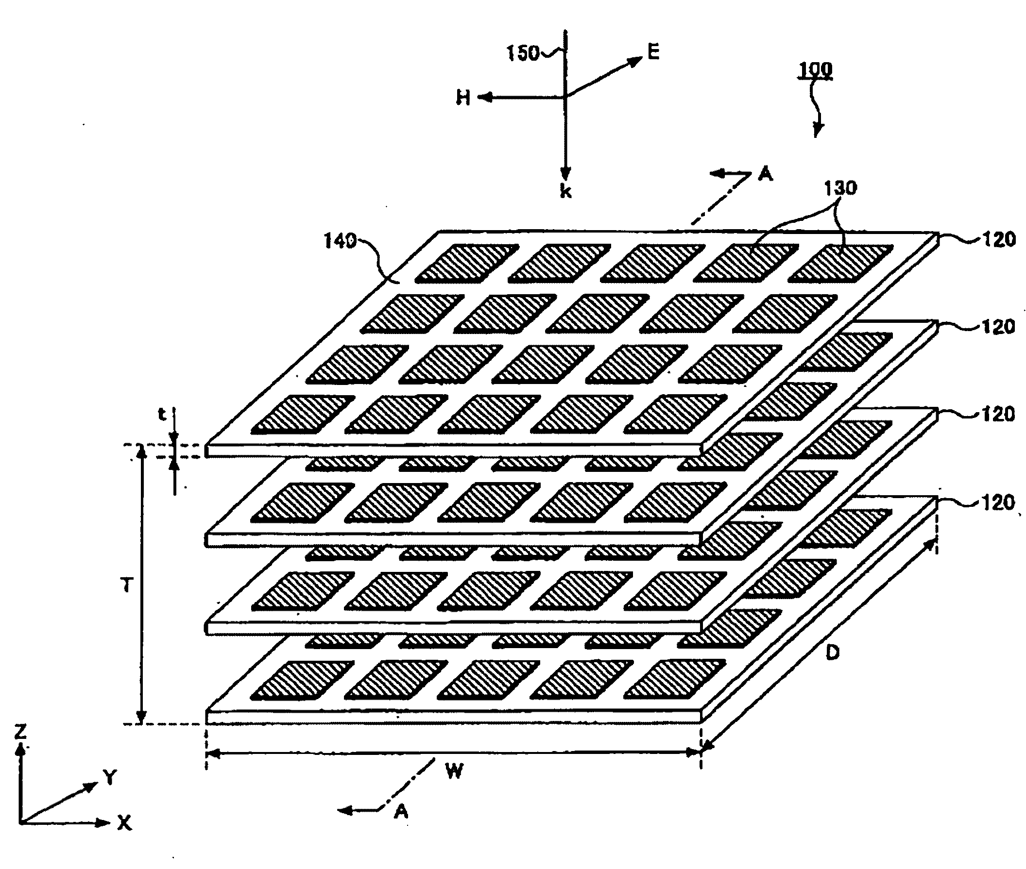
[0102]FIG. 3 shows a perspective view illustrating an example of a configuration of the artificial medium according to the invention. In addition, FIG. 4 shows an enlarged view illustrating the conductive elements which are disposed on the conductive surface of the dielectric layer constituting the artificial medium according to the invention.
[0103]As shown in FIG. 3, the artificial medium 100 according to the invention is substantially configured such that plural dielectric layers 120 with a length W (the length in the X direction shown in FIG. 3), a width D (the length in the Y direction shown in FIG. 3), and a thickness t (the length in the Z direction shown in FIG. 3) are laminated along the thickness direction. Here, in FIG. 3, in order to clarify the description, the artificial medium is illustrated as an exploded view in which the respective dielectric layers 120 are separated. However, in a real medium according to the invention, it should be noted that the respective dielec...
second embodiment
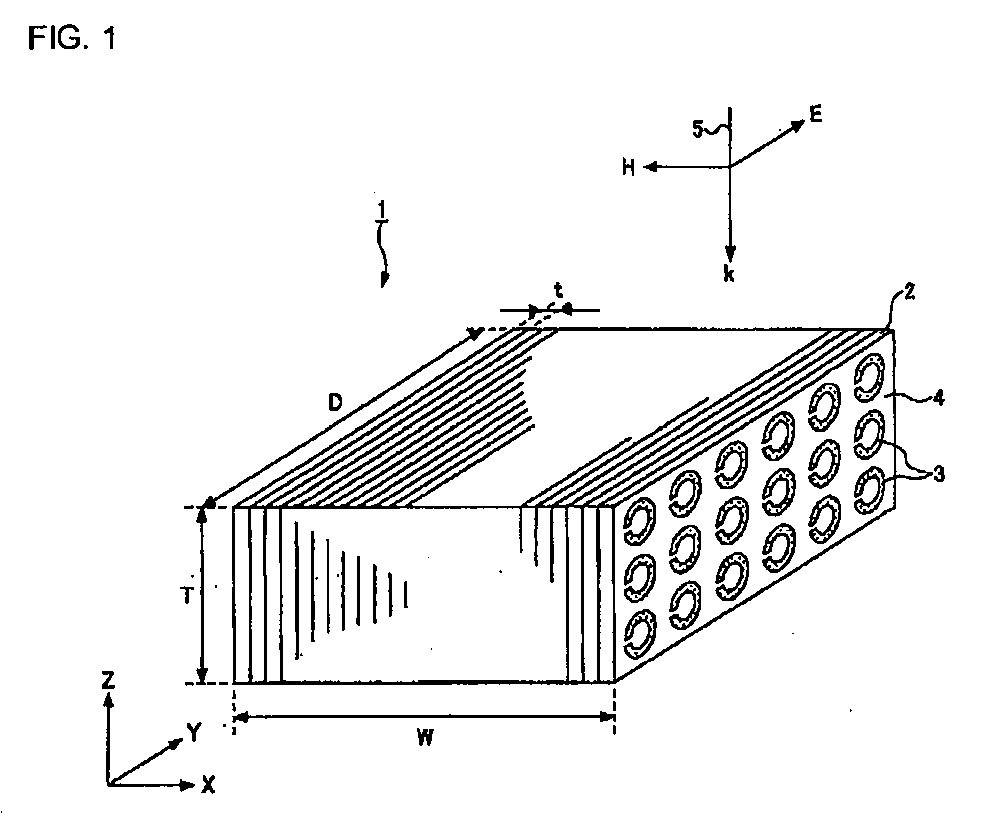
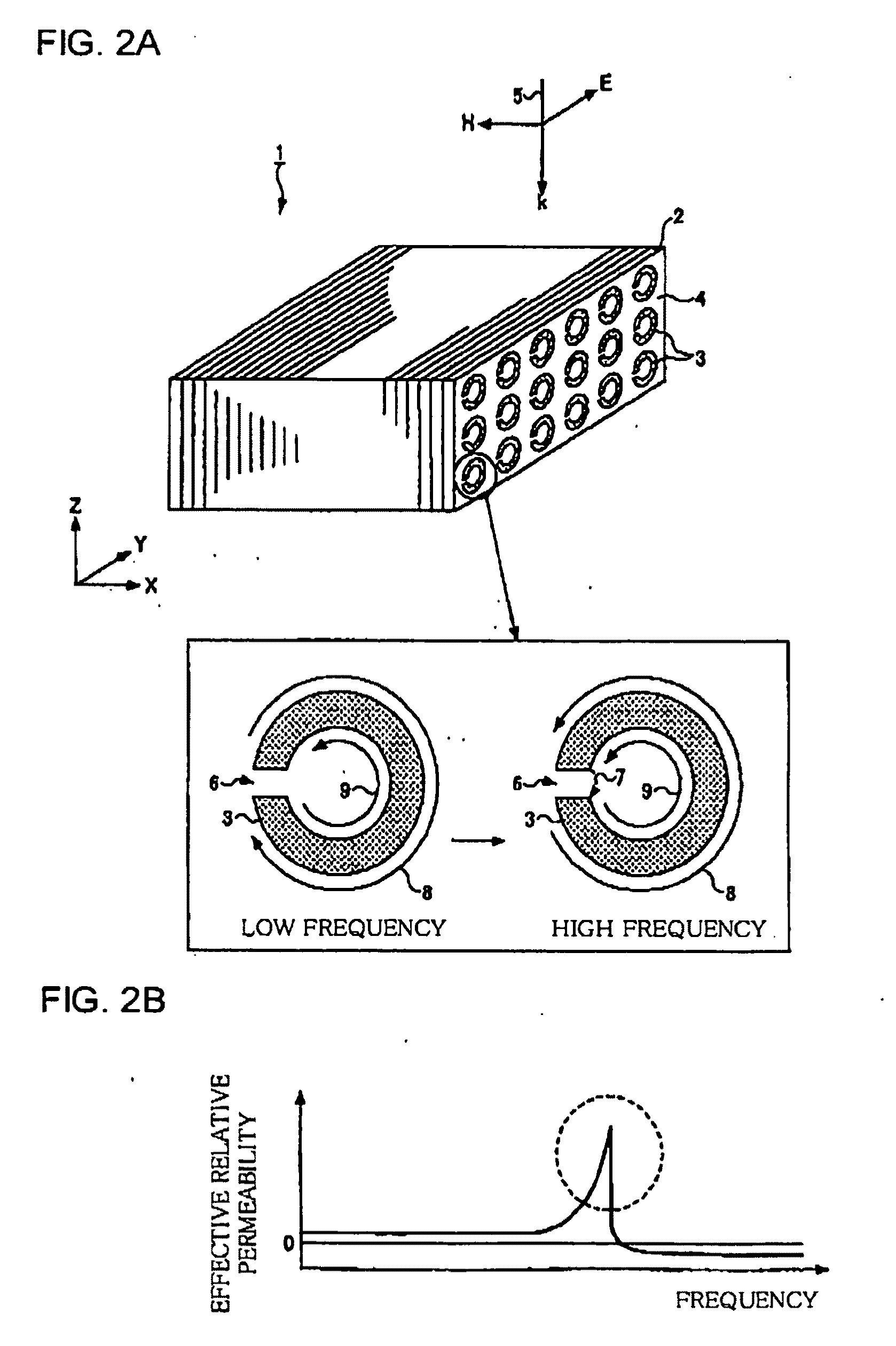
[0122]Next, an example of a configuration of the artificial medium according to the second embodiment of the invention will be described with reference to FIGS. 10A and 10B. FIG. 10A is a top view of the artificial medium 800, and FIG. 10 is a cross-sectional view taken along the line B-B.
[0123]Similar to the above-mentioned artificial medium 100, the artificial medium 800 is configured such that plural dielectric layers 820 each having the conductive surface 840 are laminated. In addition, on the conductive surface 840, plural conductive elements 830 are disposed as described above. In this case, the artificial medium 800 is different from the above-mentioned artificial medium 100 in that plural linear conductor elements 860 are provided in each dielectric layer 820. Further, the linear conductor element 860 may be made of the same material as that of the conductive element 830.
[0124]The respective linear conductor elements 860 have substantially the same line width d1 (length in t...
third embodiment
[0140]Hereinbefore, the invention has been described as an example of the artificial medium, which is configured such that two or more conductive surfaces are laminated thereon in a thickness direction, and each of which is provided with conductive elements in a two-dimensional periodic array. However, the artificial medium according to the invention is not limited to such a configuration. That is, even with an artificial medium in which a single conductive element is disposed on each conductive surface, the above-mentioned effect can be obtained.
[0141]Hereinafter, an example of the artificial medium having the above-mentioned configuration according to the third embodiment of the invention will be described in detail with reference to FIGS. 18A to 20. Here, FIG. 18A is a top view illustrating the artificial medium 900 according to the third embodiment of the invention. FIG. 18B is a cross-sectional view of the artificial medium 900 taken along the line G-G. In addition, FIGS. 19 an...
PUM
| Property | Measurement | Unit |
|---|---|---|
| Angle | aaaaa | aaaaa |
| Length | aaaaa | aaaaa |
| Length | aaaaa | aaaaa |
Abstract
Description
Claims
Application Information