Wavelength tunable interference filter, method of manufacturing wavelength tunable interference filter, optical apparatus, and optical component

a wavelength tunable interference and filter technology, applied in the field of wavelength tunable interference filters, can solve the problems of inevitable damage to the wire group of the array substrate, problems occurring in the method of manufacturing a liquid crystal display body, etc., and achieve the effect of preventing damage and breakage of the wire group

Active Publication Date: 2014-04-03
SEIKO EPSON CORP
View PDF1 Cites 7 Cited by
  • Summary
  • Abstract
  • Description
  • Claims
  • Application Information

AI Technical Summary

Benefits of technology

[0007]An advantage of some aspects of the invention is to provide a wavelength tunable interference filter capable of preventing damage to and breakage of a wire group due to a breaking portion, a method of manufacturing the wavelength tunable interference filter, an optical apparatus and an optical component using the wavelength tunable interference filter.

Problems solved by technology

Accordingly, problems occurring in the method of manufacturing a liquid crystal display body may also occur in the manufacturing of the wavelength tunable interference filter.
Accordingly, when the interference of the color filter breaking portion exceeding the setting value (assumed value) occurs, damage to the wire group of the array substrate has been inevitable.

Method used


Image

  • Wavelength tunable interference filter, method of manufacturing wavelength tunable interference filter, optical apparatus, and optical component
  • Wavelength tunable interference filter, method of manufacturing wavelength tunable interference filter, optical apparatus, and optical component
  • Wavelength tunable interference filter, method of manufacturing wavelength tunable interference filter, optical apparatus, and optical component

Examples


first embodiment

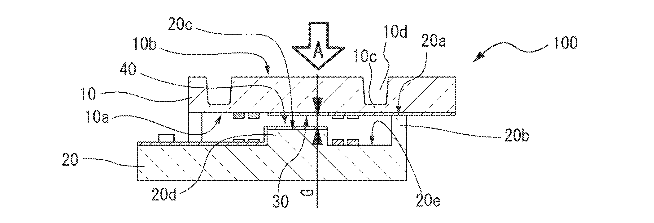
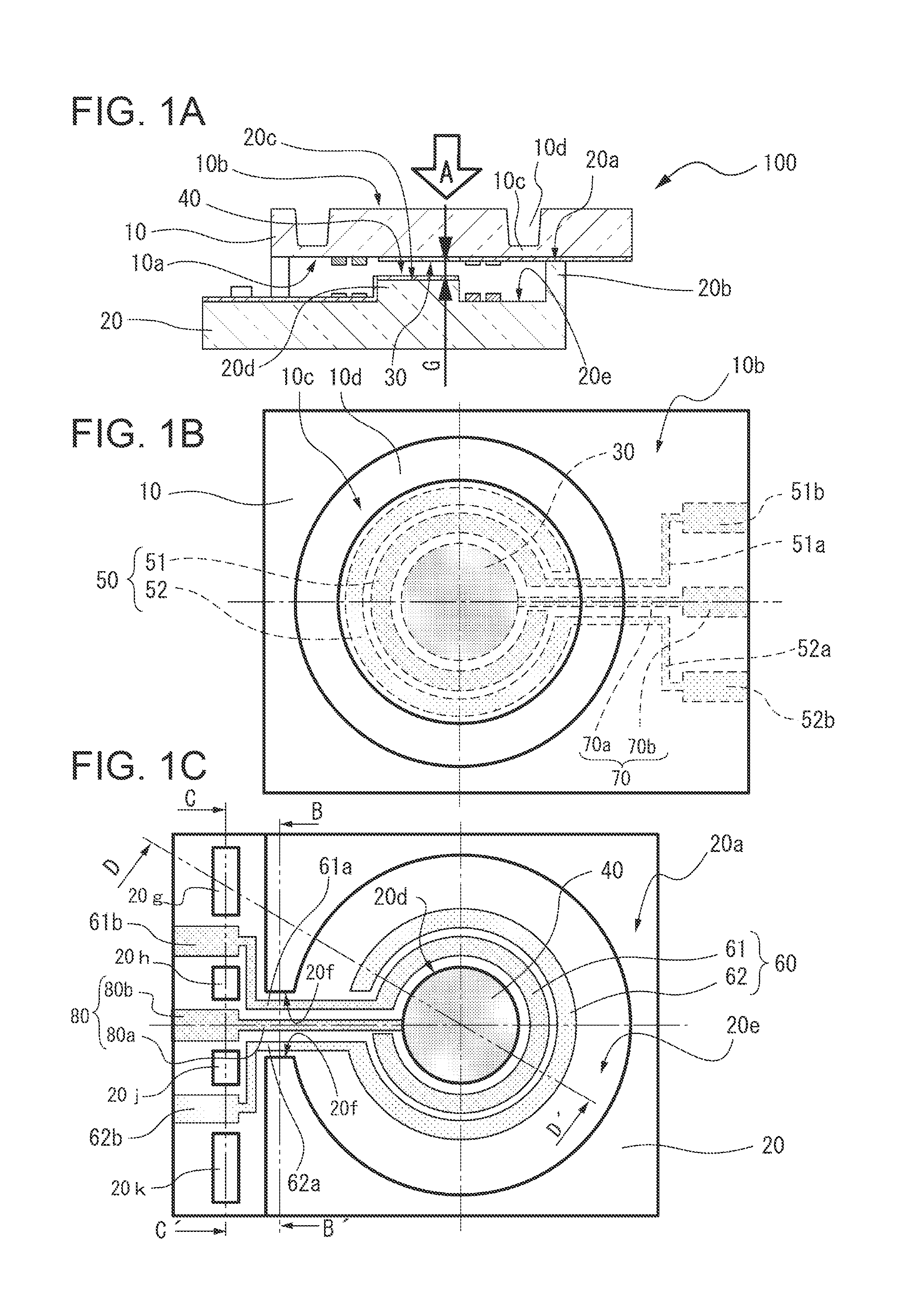
[0055]FIG. 1A schematically shows a variable gap etalon filter capable of controlling a gap between optical films as an example of a wavelength tunable interference filter according to a first embodiment. As shown in FIG. 1A, a variable gap etalon filter 100 (hereinafter, referred to as an etalon filter 100) as a wavelength tunable interference filter according to the present embodiment is configured to include a first substrate 10 formed of a light transmissive material, for example, various kinds of glass, such as soda glass, crystalline glass, quartz glass, lead glass, potassium glass, and alkali-free glass, or crystal and a second substrate 20 including a support portion 20b that has a bonding surface 20a, which is bonded to the first substrate 10, on the end surface.

[0056]FIG. 1B is a plan view of the first substrate 10 when viewed from the direction of the arrow A shown in FIG. 1A. As shown in FIGS. 1A and 1B, a first optical film 30 having both transmission and reflection cha...

second embodiment

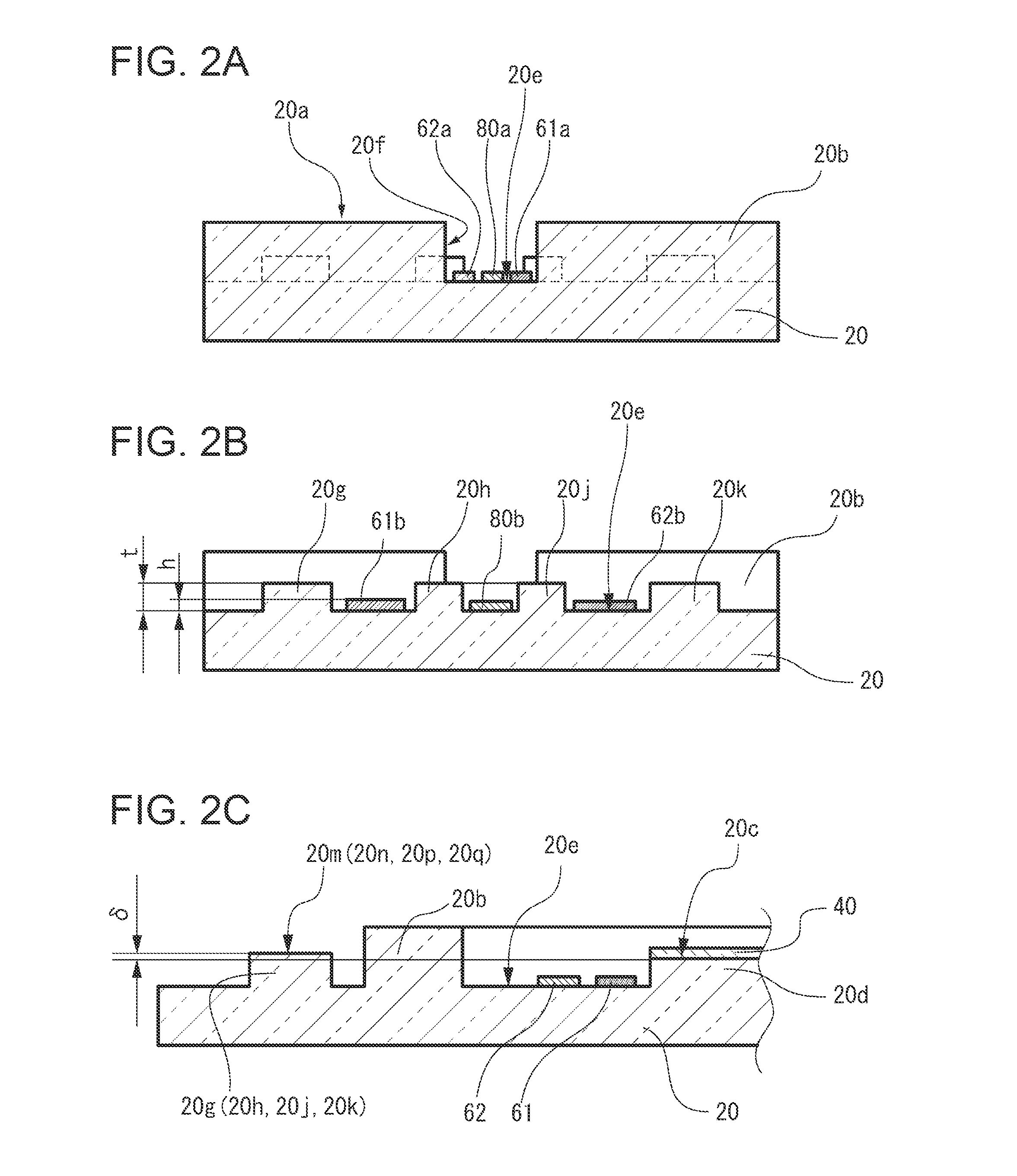
[0067]FIG. 3A is a schematic cross-sectional view showing an etalon filter 200 according to a second embodiment, FIG. 3B is a plan view of a first substrate 11 when viewed from the direction of the arrow E shown in FIG. 3A, and FIG. 3C is a cross-sectional view taken along the line F-F′ of FIG. 3B. The etalon filter 200 according to the second embodiment is different from the etalon filter 100 according to the first embodiment in that the protruding portions 20g, 20h, 20j, and 20k provided on the second substrate 20 of the etalon filter 100 are disposed on the first substrate 11. Therefore, in the etalon filter 200 according to the second embodiment, the same components as in the etalon filter 100 according to the first embodiment are denoted by the same reference numerals, and explanation thereof will be omitted.

[0068]As shown in FIG. 3A, the etalon filter 200 is configured to include a first substrate 11 and a second substrate 21 including a support portion 21b that has a bonding ...

third embodiment

[0071]FIG. 4 is a flowchart showing a method of manufacturing the etalon filter 100 according to a third embodiment. First, the first substrate 10 will be described.

First Wafer Manufacturing Process

[0072]The first wafer manufacturing process is a process of forming a collection of a plurality of first substrates 10 on a wafer of a substrate material, and includes the following steps.

Step of Preparing a Wafer for a First Substrate

[0073]First, in a step of preparing a wafer for a first substrate (S11), a first wafer 1000 of a substrate material shown in a cross-sectional view of FIG. 5A, which has a predetermined thickness and of which both surfaces 1000a and 1000b have been mirror-polished flat, is prepared, and pretreatment including predetermined washing and the like is performed.

Diaphragm Portion Forming Step

[0074]For the prepared first wafer 1000, the process proceeds to a diaphragm portion forming step (S12). In the diaphragm portion forming step (S12), as shown in FIG. 5B, an e...


PUM


Abstract

A wavelength tunable interference filter, an optical apparatus, and an optical component include a first substrate, which includes a first optical film and a first driving electrode, and a second substrate, which includes a support portion that supports the first substrate, a second optical film, and a second driving electrode. The second substrate includes an external connection electrode extending to an outer side of the support portion, and includes an electrode forming surface on which the external connection electrode is disposed. A plurality of protruding portions protruding from the electrode forming surface are formed so as to be arrayed in a direction crossing the extending direction of the external connection electrode.

Description

BACKGROUND[0001]1. Technical Field[0002]The present invention relates to a wavelength tunable interference filter, a method of manufacturing a wavelength tunable interference filter, an optical apparatus, and an optical component.[0003]2. Related Art[0004]As a method of manufacturing a wavelength tunable interference filter, a method of forming first and second reflective films that form a Fabry-Perot resonator on first and second substrates, respectively, and bonding the first and second substrates to each other can be considered. In this case, it is possible to manufacture a first wafer as a collection of a plurality of first substrates and a second wafer as a collection of a plurality of second substrates, bond the first and second wafers to each other to form a collection of a plurality of devices, and finally separate the collection of the plurality of devices into individual devices using a method called dicing, which is a cutting method using a grindstone, or breaking by bend...

Claims


Application Information

Patent Timeline
Patent Type & Authority Applications(United States)
IPC IPC(8): G02B5/28
CPCG02B5/28G02B26/001
Inventor SHINTO, SUSUMU
Owner SEIKO EPSON CORP
Why Eureka
Try Eureka