Printed circuit board having DC blocking dielectric waveguide vias
- Summary
- Abstract
- Description
- Claims
- Application Information
AI Technical Summary
Benefits of technology
Problems solved by technology
Method used
Image
Examples
Embodiment Construction
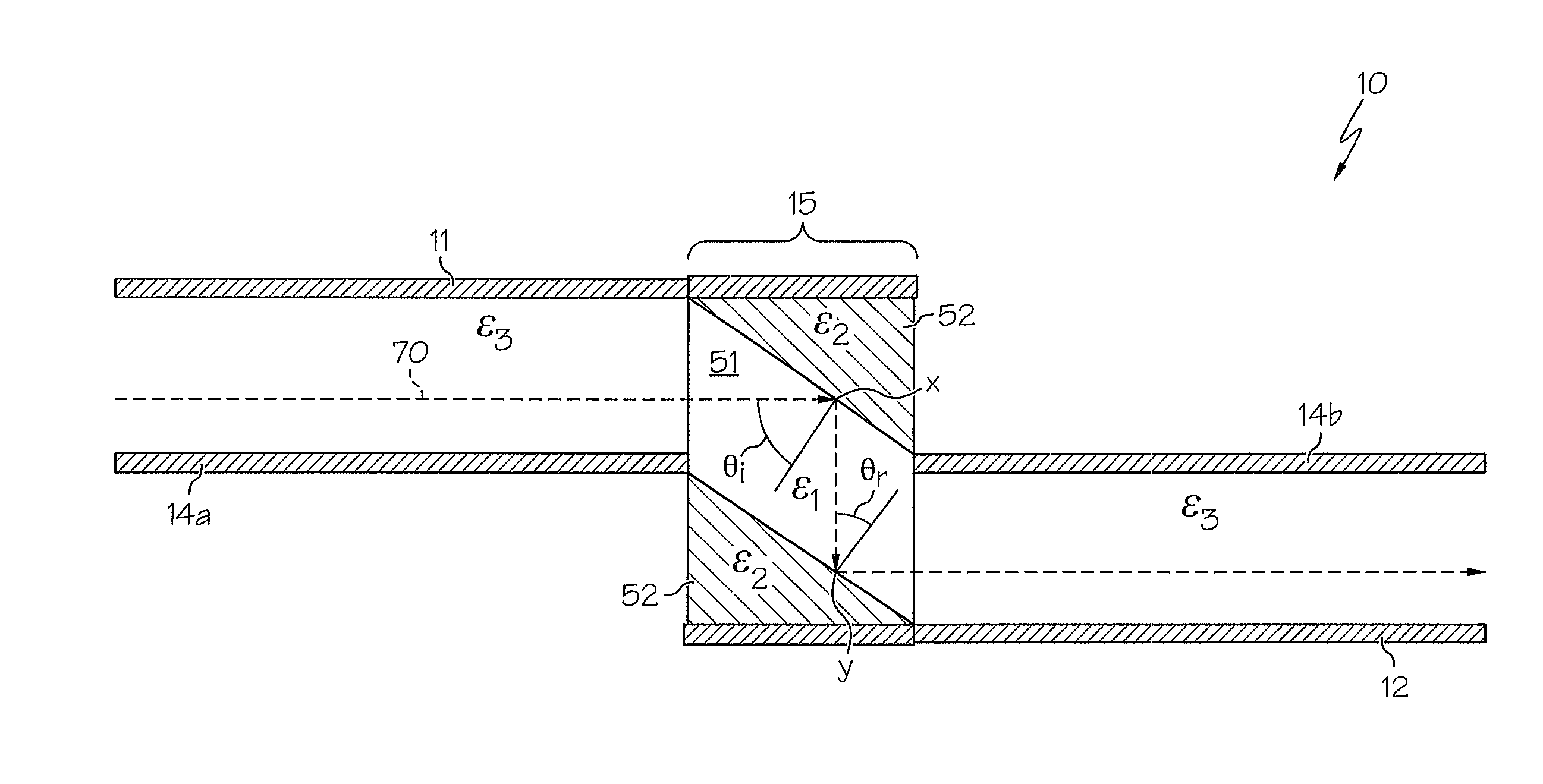
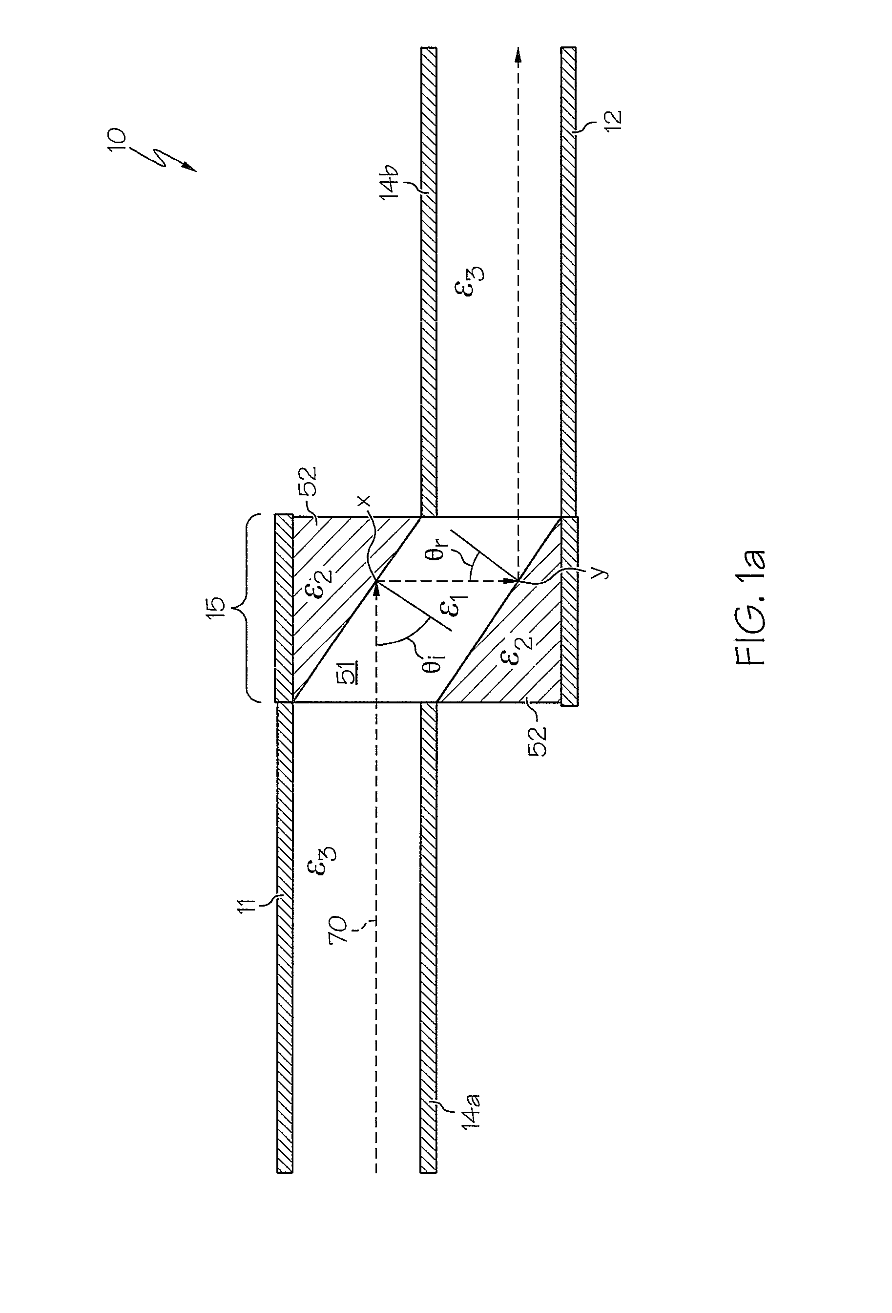
[0013]Referring now to the drawings and in particular to FIG. 1a, there is illustrated a diagram of a printed circuit board (PCB) having a dielectric waveguide via, in accordance with a preferred embodiment of the present invention. As shown, a PCB 10 includes a first microstrip 11, a second microstrip 12 and a dielectric waveguide via 15. PCB 10 also includes ground planes 14a, 14b. First microstrip 11 and ground plane 14a are connected to second microstrip 12 and ground plane 14b by dielectric waveguide via 15.
[0014]Microstrips 11, 12 and ground planes 14a, 14b are preferably made of copper layers. The area of PCB 10 that is located between microstrip 11 and ground plane 14a is made of dielectric material having a dielectric constant ε3. Similarly, the area of PCB 10 that is located between ground plane 14b and microstrip 12 is made of dielectric material having a. dielectric constant ε3.
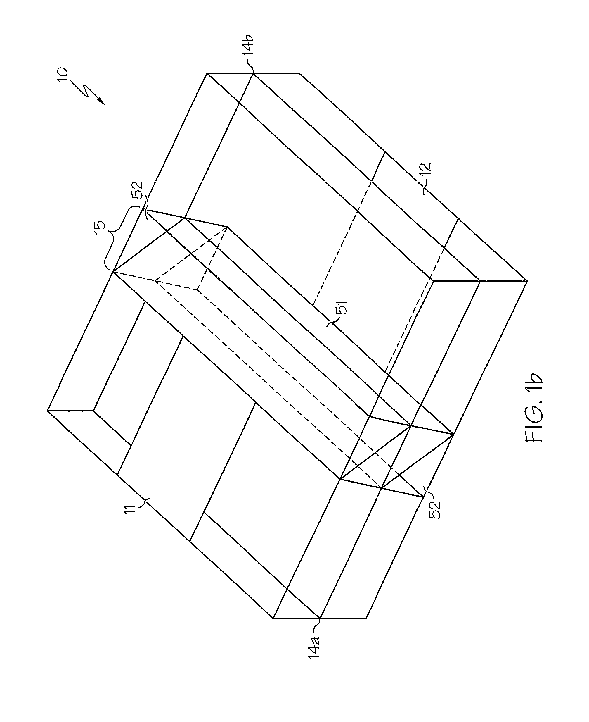
[0015]An isometric view of PCB 10 is depicted in FIG. 1b. Since microstrip 11 is not connected...
PUM
| Property | Measurement | Unit |
|---|---|---|
| Dielectric polarization enthalpy | aaaaa | aaaaa |
| Angle | aaaaa | aaaaa |
| Magnetism | aaaaa | aaaaa |
Abstract
Description
Claims
Application Information


