
Multilevel converter circuit

Active Publication Date: 2014-04-10
FUJI ELECTRIC CO LTD
View PDF7 Cites 27 Cited by
  • Summary
  • Abstract
  • Description
  • Claims
  • Application Information

AI Technical Summary

Benefits of technology

The invention aims to reduce loss and improve efficiency in a device by controlling the number of semiconductor switches through which output current passes. This allows for a more direct current input power source, which can be combined from two single sources, leading to lower operational restrictions and easier fabrication of the device. Ultimately, this results in higher efficiency, price reduction, and miniaturization of the device.

Problems solved by technology

With the circuits of FIGS. 23 and 24, the number of semiconductor switches through which output current passes is a maximum of six in series or a maximum of eight in series between the direct current combined power source BA2 of each circuit and the alternating current output point U. Because of this, steady on loss in the semiconductor switches increases, thus causing a decrease in the efficiency of the whole of the device, and leading to a difficulty in miniaturization and price reduction.
Because of this, as six or eight single power sources which can supply powers independently are necessary for the direct current combined power source BA2 which is an input, this brings about a big restriction on manufacturing the device.

Method used


Image

  • Multilevel converter circuit
  • Multilevel converter circuit
  • Multilevel converter circuit

Examples


Embodiment Construction

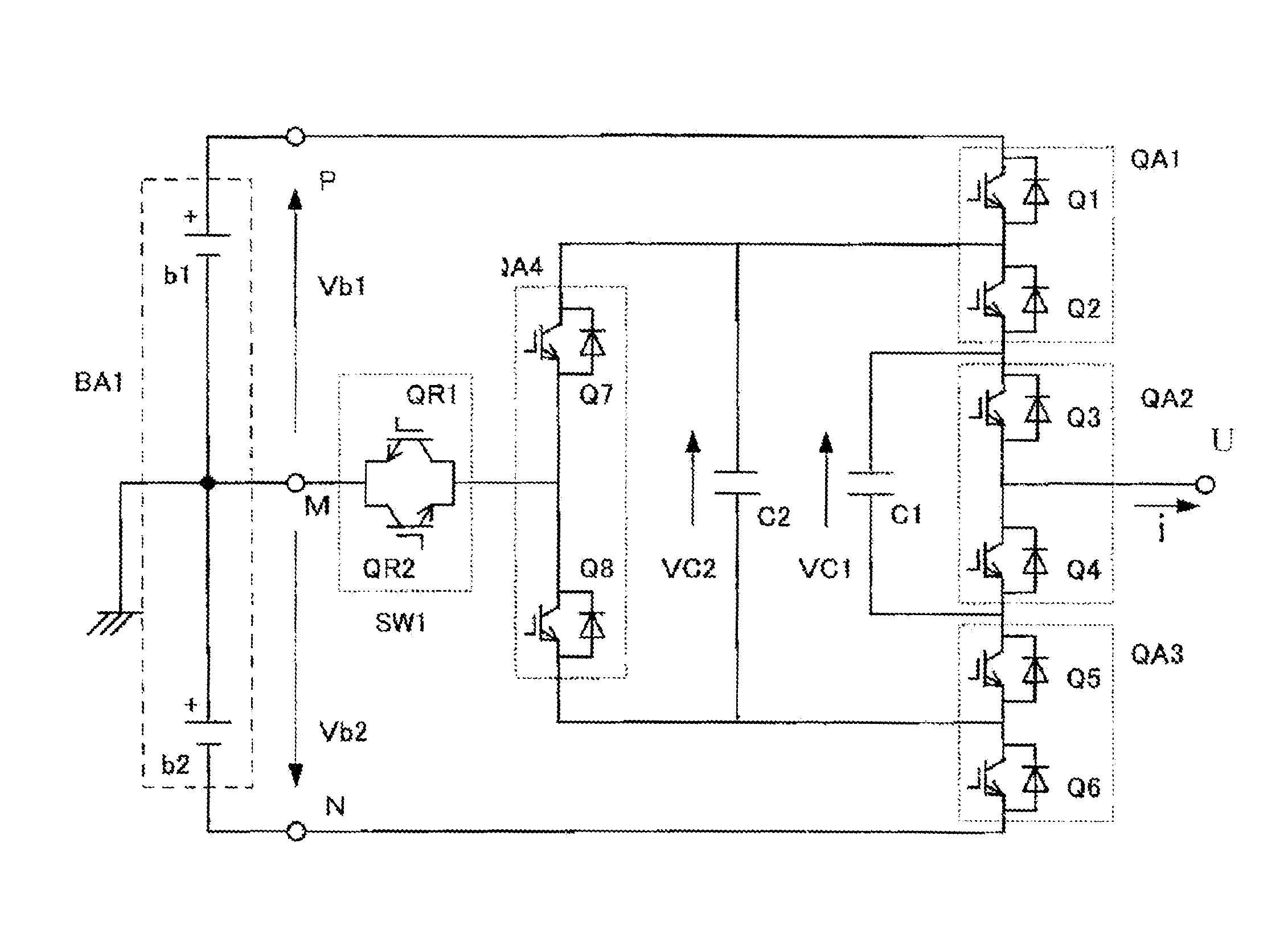
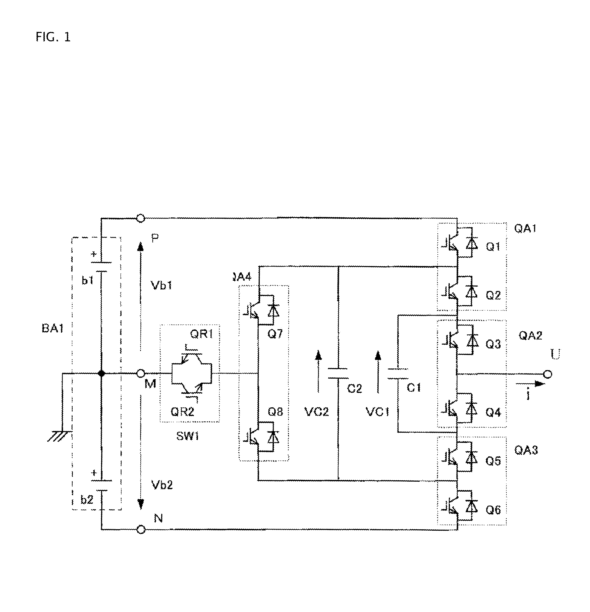
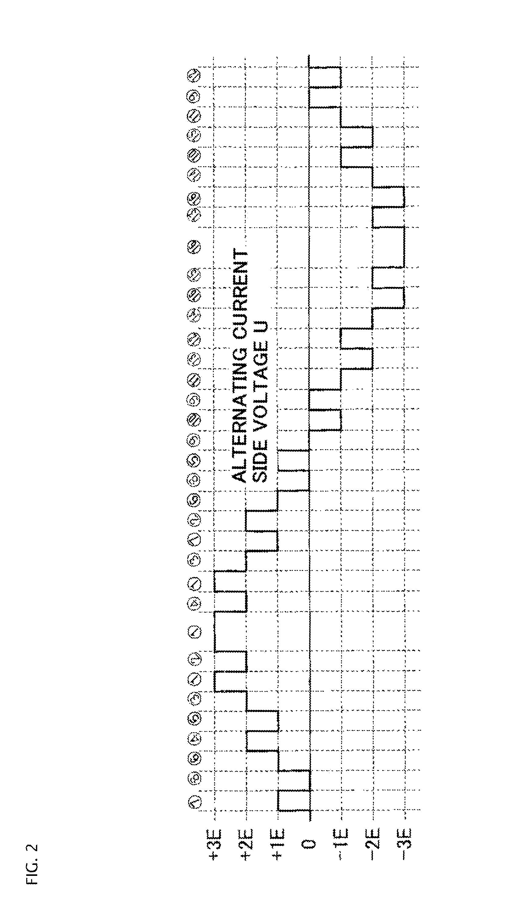
[0072]FIG. 1 is a circuit diagram showing an embodiment of the invention, FIG. 2 is an example diagram of a seven-level output waveform in FIG. 1, and FIG. 3 is an illustration of switching patterns in FIG. 1.

[0073]A direct current combined power source (also referred to simply as a direct current power source) BA1 is shown here as one, with direct current single power sources b1 and b2 connected in series, having three terminals, a positive terminal P, a negative terminal N, and a zero terminal (a ground terminal) M. An arm pair QA1 formed of semiconductor switches Q1 and Q2, an arm pair QA2 formed of semiconductor switches Q3 and Q4, and furthermore, an arm pair QA3 formed of semiconductor switches Q5 and Q6 are connected in series to the direct current power source BA1. Also, the outer side terminals of an arm pair QA4 formed of semiconductor switches Q7 and Q8 are connected between the midpoint terminal of the arm pair QA1 and the midpoint terminal of the arm pair QA3, and an al...


PUM


Abstract

In some aspects of the invention, a number of semiconductor switches through which output current passes can be reduced between a direct current power source side, which is an input, and an alternating current output, thus achieving loss reduction, and enabling higher efficiency, price reduction, and miniaturization of a device. In some aspects, a direct current power source, formed of a series connection circuit of single power sources, which has three mutually different voltage levels including zero can be provided with first, second, third, and fourth arm pairs, each configured by connecting two arms formed of semiconductor switches in series, an alternating current switch configured by combining semiconductor switches. As such, a plurality of voltage levels can be to be selected from and output by an on and off control of these switch elements.

Description

CROSS-REFERENCE TO RELATED APPLICATIONS[0001]This application is a continuation of International Application No. PCT / JP2012 / 63508, filed on May 25, 2012, which is based on and claims priority to Japanese Patent Application No. JP 2011-149269, filed on Jul. 5, 2011. The disclosure of the Japanese priority application and the PCT application in their entirety, including the drawings, claims, and the specification thereof, are incorporated herein by reference.BACKGROUND[0002]1. Field of the Invention[0003]Embodiments of the invention relate to multilevel converter circuits.[0004]2. Related Art[0005]FIG. 23 shows one phase's worth of seven-level converter circuit disclosed in, for example, Japanese Patent Application No. JP-A-11-164567 (also referred to herein as “PTL 1”).[0006]A series circuit of semiconductor switches Q1 to Q12 is connected between the positive terminal and negative terminal of a direct current combined power source BA2 wherein direct current single power sources b11 ...

Claims


Application Information

Patent Timeline
IPC IPC(8): H02M7/537
CPCH02M7/537H02M7/483H02M7/487H02M1/36
Inventor YATSU, MAKOTO
Owner FUJI ELECTRIC CO LTD
Learn More