Mask for bumping solder balls on circuit board and solder ball bumping method using the same

a solder ball and circuit board technology, applied in the direction of non-electric welding apparatus, manufacturing tools, soldering apparatus, etc., can solve the problems of low productivity, high viscosity flux, and the solder ball is not connected to the i/o pad of the substra

Inactive Publication Date: 2014-04-17
SAMSUNG ELECTRO MECHANICS CO LTD
View PDF1 Cites 53 Cited by
  • Summary
  • Abstract
  • Description
  • Claims
  • Application Information

AI Technical Summary

Benefits of technology

[0029]In the removing of the mask, the flux

Problems solved by technology

Therefore, there is a problem that the solder ball is not connected to the I/O pad of the substrate.
However, a high viscosity flux has a disadvantage in that it does not flow up to a lower portion of the solder ball 1 and the I/O pad 10 of the substrate.
As a result, productivity bec

Method used


Image

  • Mask for bumping solder balls on circuit board and solder ball bumping method using the same
  • Mask for bumping solder balls on circuit board and solder ball bumping method using the same
  • Mask for bumping solder balls on circuit board and solder ball bumping method using the same

Examples


Embodiment Construction

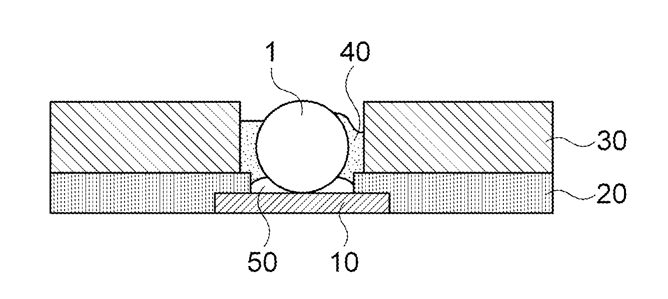
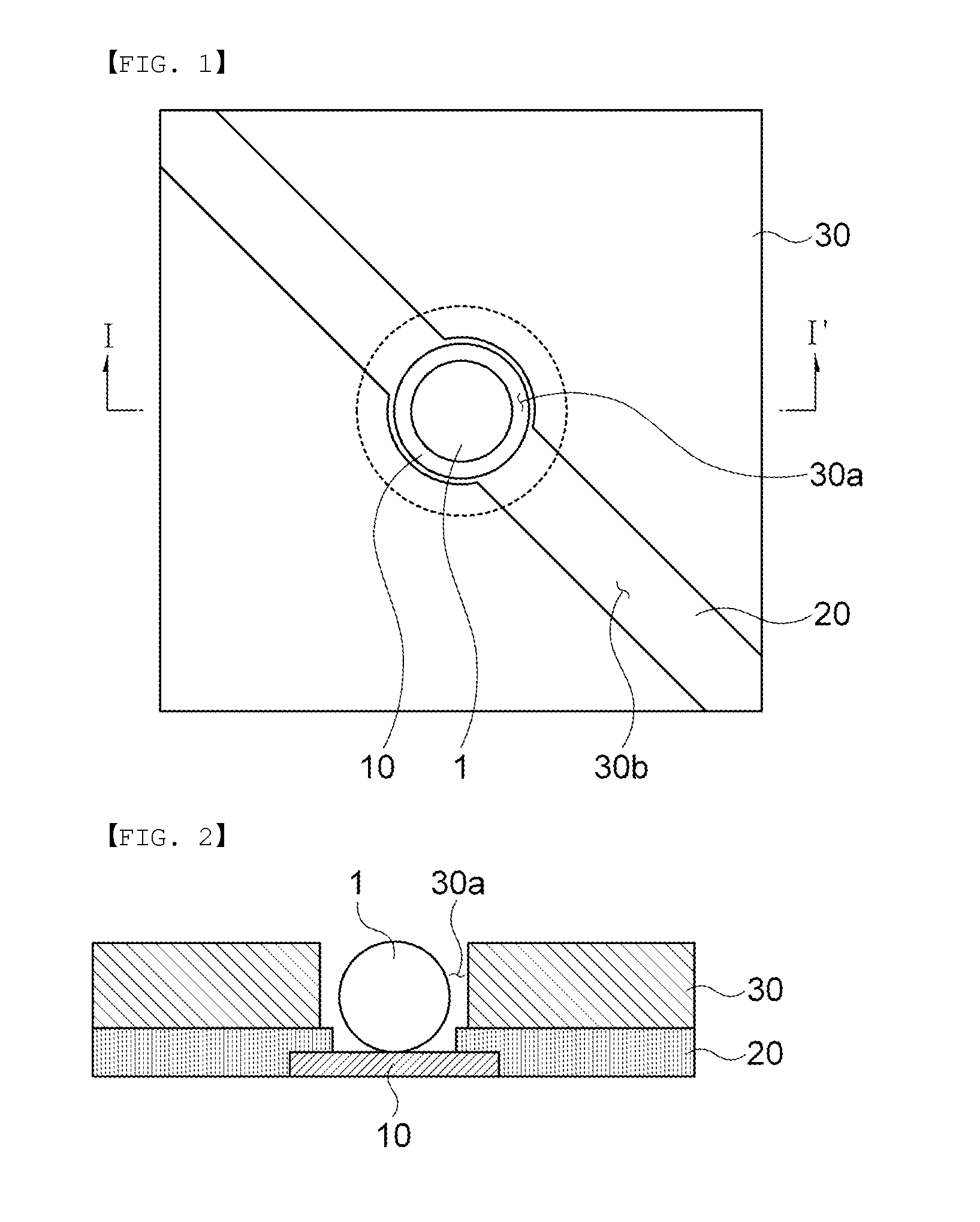
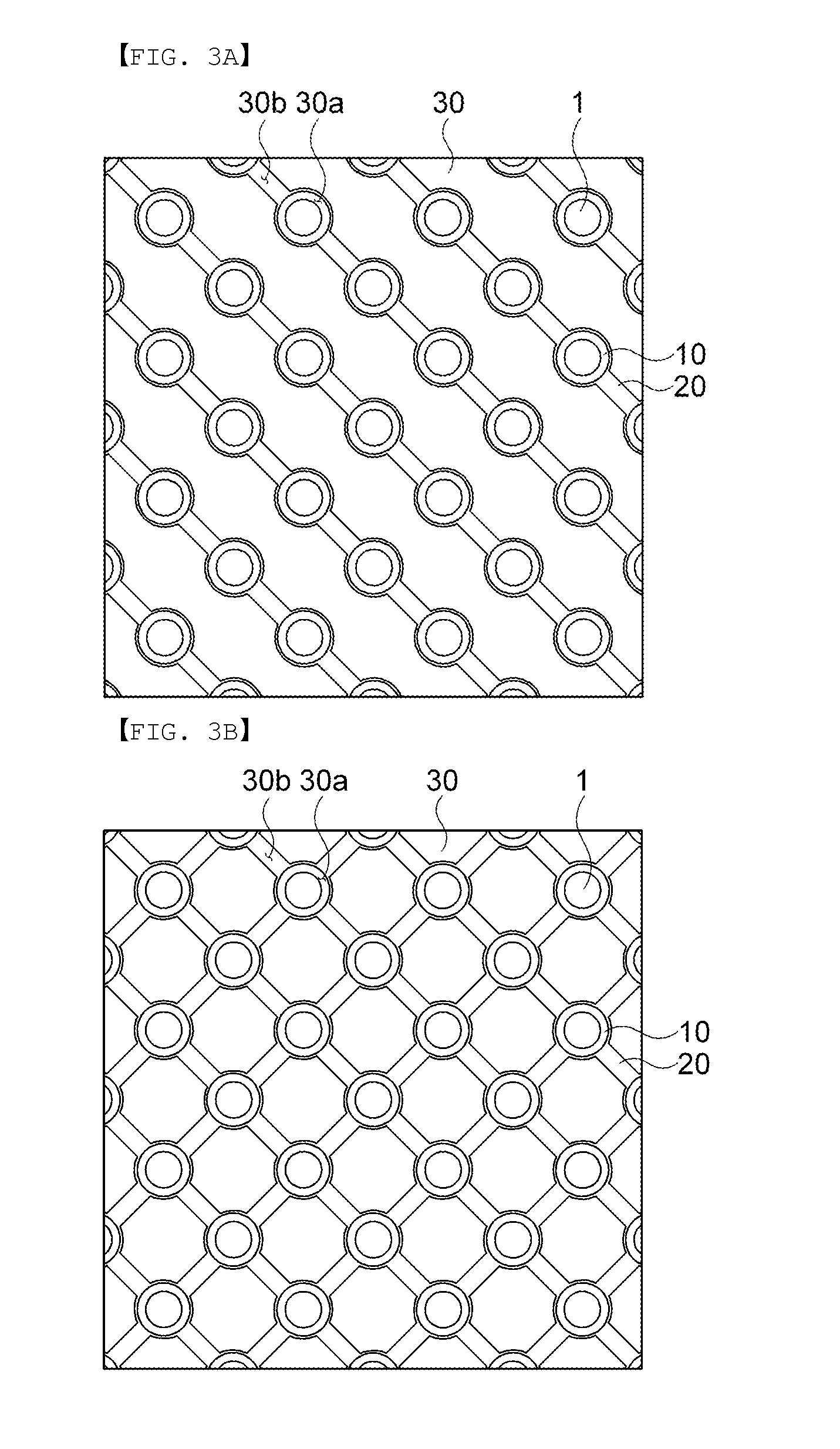
[0036]Exemplary embodiments of the present invention for accomplishing the above-mentioned objects will be described with reference to the accompanying drawings. In the present specification, the same reference numerals will be used to describe the same components, and a detailed description thereof will be omitted in order to allow those skilled in the art to easily understand the present invention.

[0037]In the specification, it will be understood that unless a term such as ‘directly’ is not used in a connection, coupling, or disposition relationship between one component and another component, one component may be ‘directly connected to’, ‘directly coupled to’ or ‘directly disposed to’ another element or be connected to, coupled to, or disposed to another element, having the other element intervening therebetween.

[0038]Although a singular form is used in the present description, it may include a plural form as long as it is opposite to the concept of the present invention and is n...


PUM

PropertyMeasurementUnit
Sizeaaaaaaaaaa
Sizeaaaaaaaaaa
Circumferenceaaaaaaaaaa

Abstract

Disclosed herein are a mask for bumping solder balls on a circuit board and a solder ball bumping method using the same. The mask includes: a plurality of openings providing spaces into which the solder balls are inserted to thereby be seated on solder pads; and trenches providing introduction spaces for spreading a flux to portions at which the solder balls are seated on the solder pads and extended from at least one side of circumferences of the openings.

Description

CROSS REFERENCE(S) TO RELATED APPLICATIONS[0001]This application claims the benefit under 35 U.S.C. Section 119 of Korean Patent Application Serial No. 10-2012-0112966, entitled “Mask for Bumping Solder Balls on Circuit Board and Solder Ball Bumping Method Using the Same” filed on Oct. 11, 2012, which is hereby incorporated by reference in its entirety into this application.BACKGROUND OF THE INVENTION[0002]1. Technical Field[0003]The present invention relates to a mask for bumping solder balls on a circuit board and a solder ball bumping method using the same, and more particularly, to a mask for bumping a solder ball on a circuit board including a trench so as to provide an introduction space for spreading a flux, and a solder ball bumping method using the same.[0004]2. Description of the Related Art[0005]Recently, application of a flip chip scheme of forming a solder bump on a printed circuit board (PCB) and connecting a device onto the solder bump has gradually increased. Particu...

Claims


Application Information

Patent Timeline
IPC IPC(8): B23K3/06B23K3/08
CPCB23K3/082B23K3/06H01L24/11B23K3/0623H05K3/34
Inventor CHOI, JIN WONYOU, YON HOMUN, SEON JAEMUKAI, NORIAKIKIM, SEUNG WANLEE, KIJUCHOI, JUNG IN
Owner SAMSUNG ELECTRO MECHANICS CO LTD
Why Eureka
Try Eureka