
Band Stitching Electronic Circuits and Techniques

a technology of electronic circuits and band stitching, applied in the direction of digital transmission, instruments, electrical equipment, etc., can solve the problems of impracticality or inability to convert analog signals to digital signals fast enough, and the speed limitations of the electronic components used in the receiver and the transceiver, so as to reduce the distortion of signals due to band stitching

Inactive Publication Date: 2014-04-17
RAYTHEON CO
View PDF1 Cites 45 Cited by
  • Summary
  • Abstract
  • Description
  • Claims
  • Application Information

AI Technical Summary

Benefits of technology

The present invention provides circuits and techniques for combining separate electronics band circuits while reducing signal distortion caused by band stitching. The invention includes filters and antialias filters that have complementary amplitude and phase responses in the band stitching region, resulting in a wider combined frequency band with reduced fluctuations in response. The technical effect of the invention is improved signal quality and reduced distortion in the combined signal.

Problems solved by technology

Some electronic components used in receivers and transceivers present speed limitations that influence circuit architecture.
For example, analog-to-digital converters (ADCs) used in receivers and transceivers can have speed limitations that make it impractical or impossible to convert analog signals to digital signals fast enough to allow operation over a sufficiently wide frequency band for all applications.
Stitching of bands presents particular problems for many receivers and transceivers.
The different characteristics result in undesirable signal distortions upon band stitching, particularly near the intersection of two frequency bands.
The distortions can be highly problematic, particularly when a signal, either a narrowband signal or a wideband signal, has one or more frequency components that are at or near the intersection of two adjacent frequency bands.

Method used


Image

  • Band Stitching Electronic Circuits and Techniques
  • Band Stitching Electronic Circuits and Techniques
  • Band Stitching Electronic Circuits and Techniques

Examples


Embodiment Construction

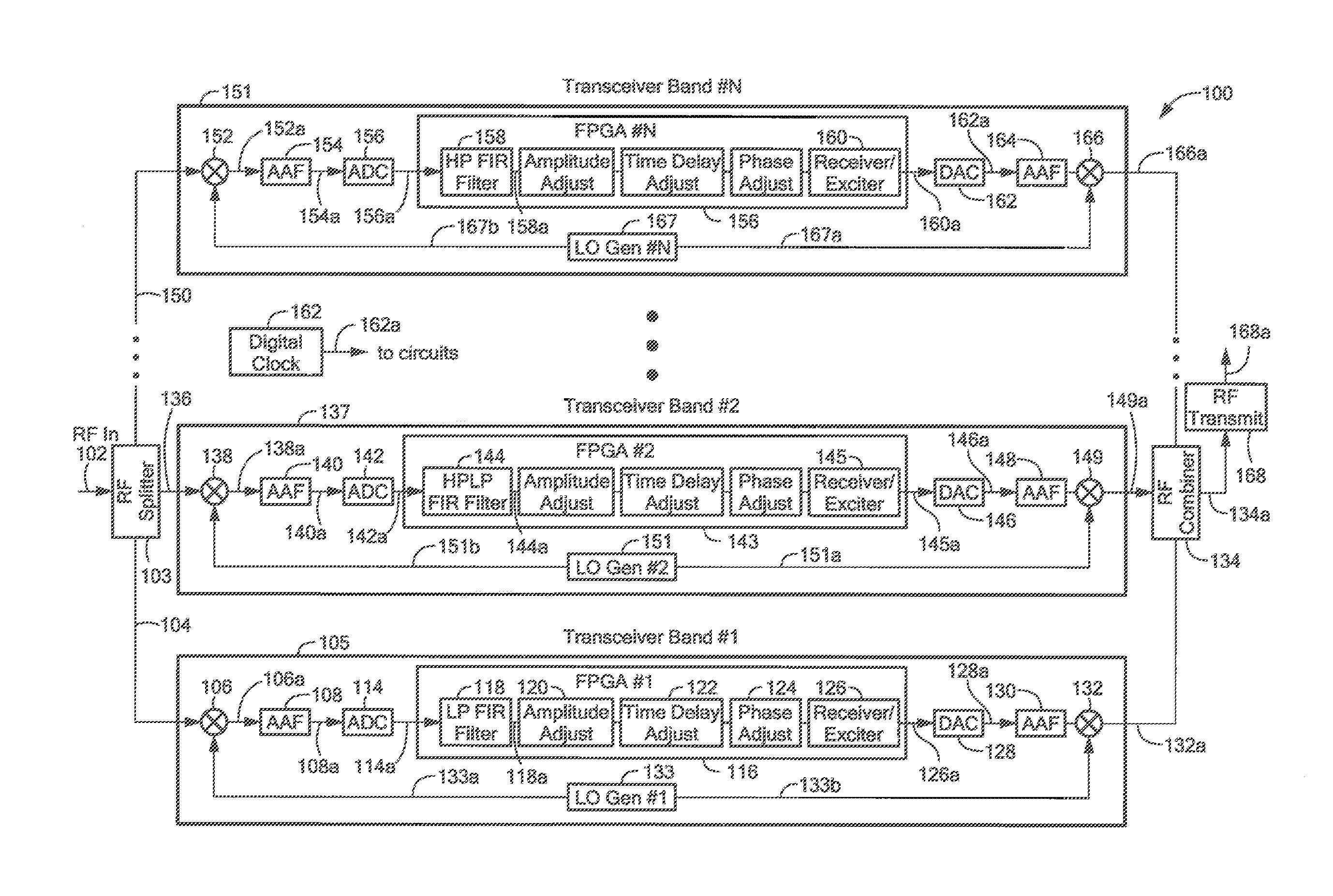
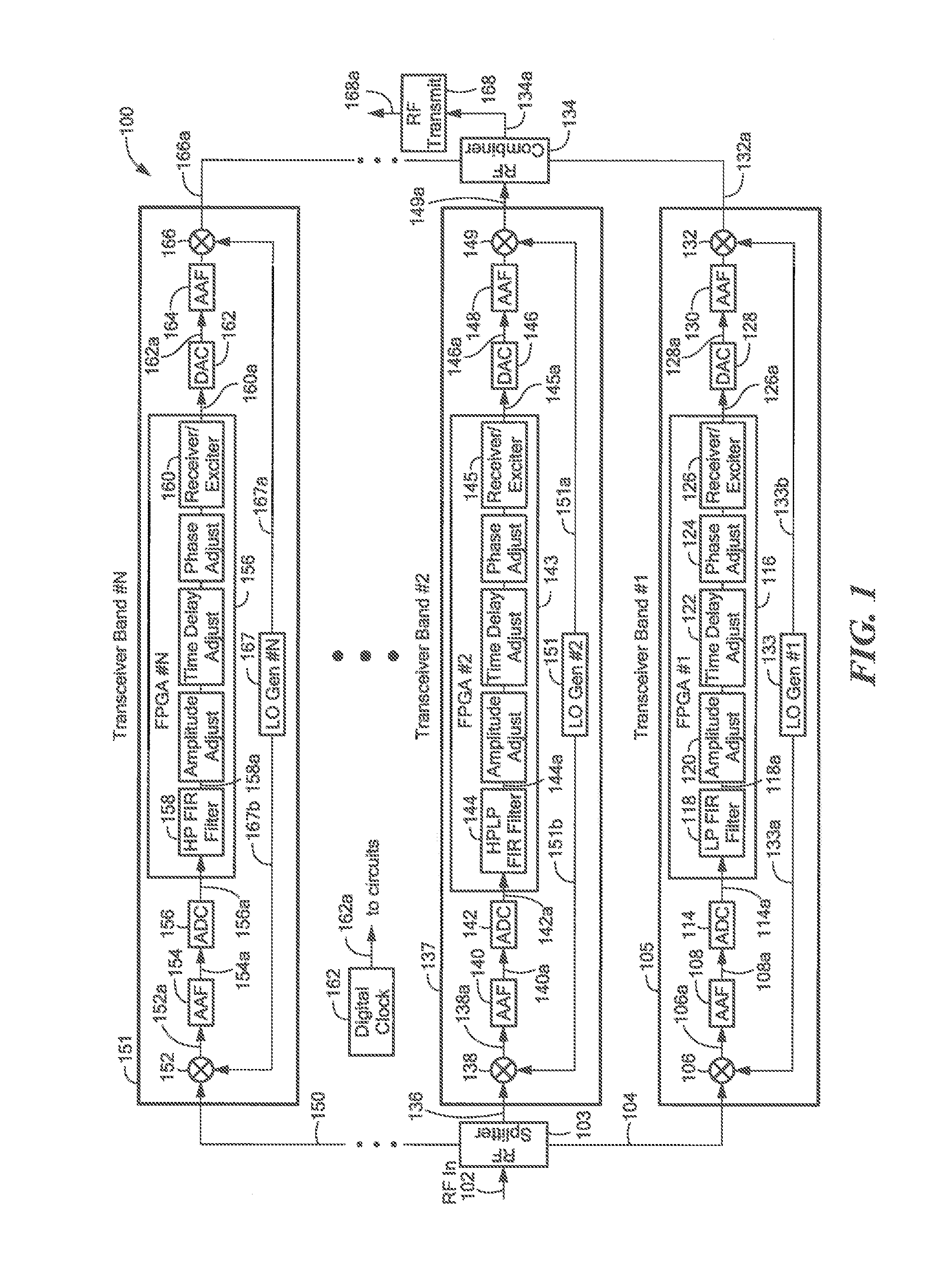
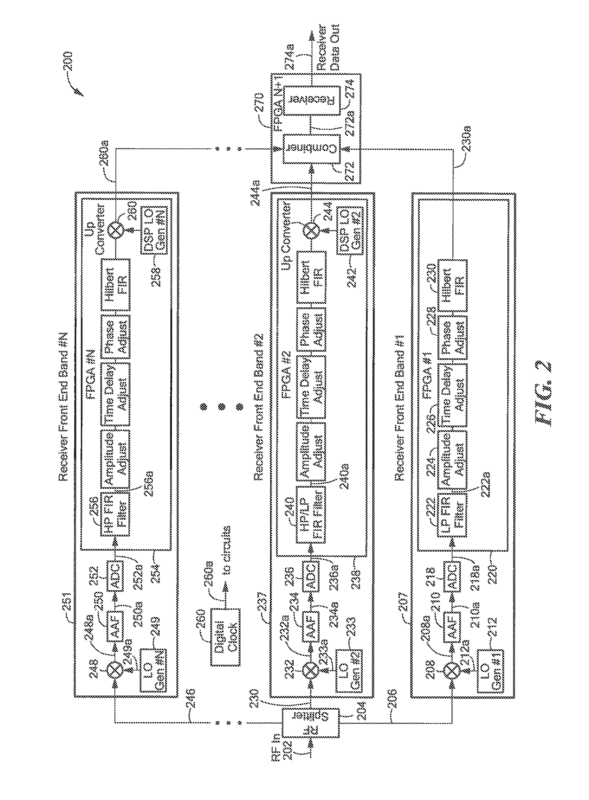
[0019]Before describing the present invention, some introductory concepts and terminology are explained. As used herein, the term “band circuit” is used to describe one of a plurality of band circuits used together in a common electronic circuit, each of which operates upon the same received radio frequency (RF) signal, but which operate in different frequency bands, i.e., upon different frequency band portions of the received radio frequency signal. The received radio frequency signal can have frequency components that can span, from time to time, or at the same time, frequencies within or throughout more than one of the frequency bands of the individual band circuits. Thus, simply stated, if an input signal has a frequency band of possible frequencies three GHz wide (e.g., centered at about 21 GHz), one band circuit can operate on the lowest one GHz of the input signal, a second band circuit can operate on the middle one GHz of the input signal, and a third band circuit can operat...


PUM


Abstract

An electronic circuit combines two or more individual wideband RF receivers or transceiver band circuits to produce a usable instantaneous bandwidth that is wider than the bandwidth of the individual band circuits. The electronic circuit overcomes the difficulties of combining bands to provide low signal distortion across the band edges and throughout the combined instantaneous bandwidth of the two or more individual band circuits. This electronic circuit utilizes an amplitude, time delay, and phase adjustment procedure that uses associated adjustable circuitry to eliminate misalignments between the two or more individual band circuits.

Description

FIELD OF THE INVENTION[0001]This invention relates generally to electronic receivers and transceivers, and, more particularly, to electronic receivers and transceivers that have a plurality of separate band circuits, each operating in separate frequency bands, signals from which are combined together into one contiguous frequency band.BACKGROUND OF THE INVENTION[0002]Radio frequency receivers and transceivers are known, including receivers and transceivers that use analog circuits, and receivers and transceivers that use both analog and digital circuits.[0003]Some electronic components used in receivers and transceivers present speed limitations that influence circuit architecture. For example, analog-to-digital converters (ADCs) used in receivers and transceivers can have speed limitations that make it impractical or impossible to convert analog signals to digital signals fast enough to allow operation over a sufficiently wide frequency band for all applications. One such applicati...

Claims


Application Information

Patent Timeline
Patent Type & Authority Applications(United States)
IPC IPC(8): H04B1/40
CPCG01S7/38H04B1/001H04B1/0057
Inventor HANEVICH, DANIEL A.FULLMER, DOUGLAS E.SAVAGE, LEE M.KAUFMAN, STEVEN L.WHITE, JACK E.
Owner RAYTHEON CO
Learn More