Apparatus for Reference Voltage Generating Circuit

a reference voltage and generating circuit technology, applied in the direction of power consumption reduction, ac network voltage adjustment, electric variable regulation, etc., can solve problems such as reliability, and achieve the effect of wide voltage range and improved scalability of inputs

Active Publication Date: 2014-04-24
STMICROELECTRONICS INT NV
View PDF8 Cites 13 Cited by
  • Summary
  • Abstract
  • Description
  • Claims
  • Application Information

AI Technical Summary

Benefits of technology

[0011]An advantage of an embodiment of the present invention is providing reference voltages for an input and output system having a wide voltage range and improving the scalability of an input and output system having a plurality of I / O interface circuits.

Problems solved by technology

When a logic signal is forwarded from an I / O interface device to a CPU, the mismatch between the supply voltages of two devices may cause a reliability issue.

Method used


Image

  • Apparatus for Reference Voltage Generating Circuit
  • Apparatus for Reference Voltage Generating Circuit
  • Apparatus for Reference Voltage Generating Circuit

Examples


Embodiment Construction

[0022]The making and using of the presently preferred embodiments are discussed in detail below. It should be appreciated, however, that the present invention provides many applicable inventive concepts that can be embodied in a wide variety of specific contexts. The specific embodiments discussed are merely illustrative of specific ways to make and use the invention, and do not limit the scope of the invention.

[0023]The present disclosure will be described with respect to embodiments in a specific context, a configurable reference voltage generating circuit for an input and output (I / O) interface circuit having a wide voltage range. The embodiments of the disclosure may also be applied, however, to a variety of reference generating circuits. Hereinafter, various embodiments will be explained in detail with reference to the accompanying drawings.

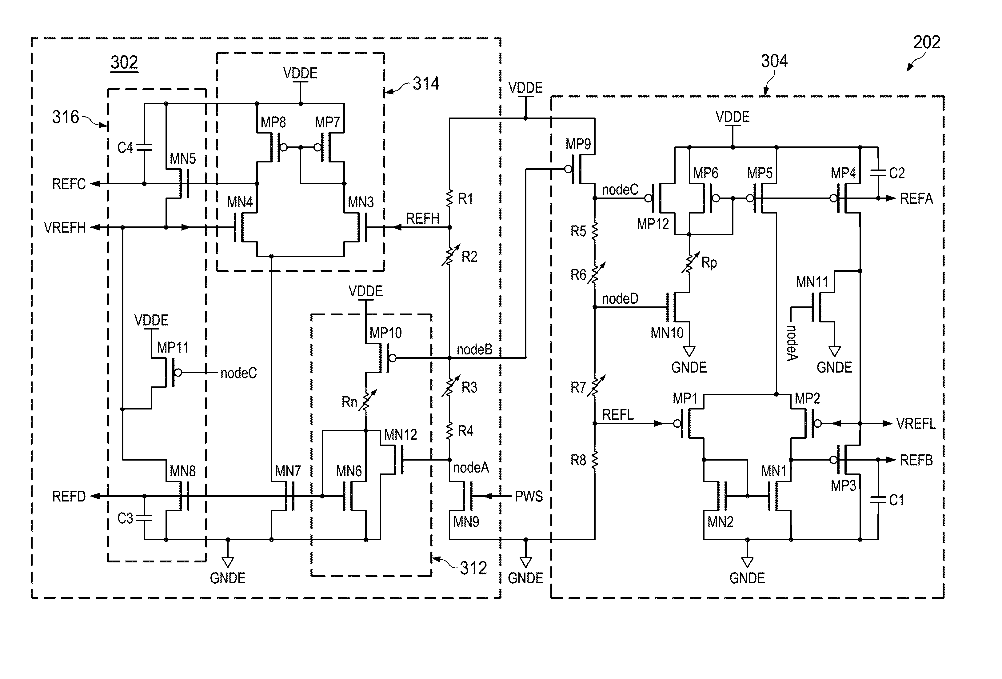
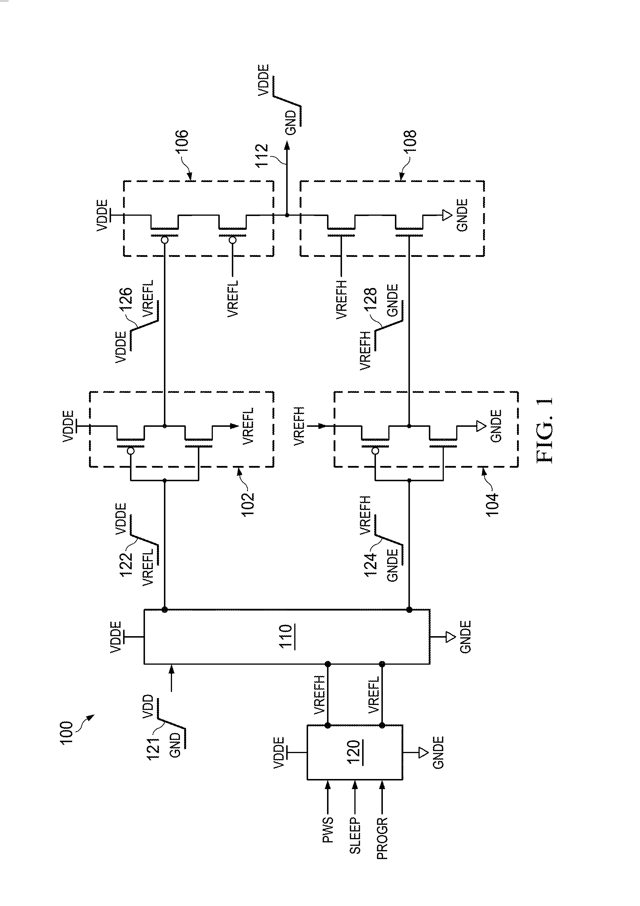
[0024]FIG. 1 illustrates a schematic diagram of an I / O interface circuit in accordance with an embodiment. The I / O interface circuit 100 ma...


PUM


Abstract

An apparatus comprises a reference voltage bias generator configured to generate a first reference voltage and a second reference voltage. During a low supply mode, the first reference voltage is equal to a supply voltage potential and the second reference voltage is equal to a ground potential. During a high supply mode, the first reference voltage is equal to a first fraction times the supply voltage potential and the second reference voltage is equal to a second fraction times the supply voltage potential. The apparatus further includes a reference voltage booster coupled to the reference voltage bias generator, wherein the reference voltage booster is configured to generate the first reference voltage and the second reference voltage with increased drive capability.

Description

TECHNICAL FIELD[0001]The present invention relates to an apparatus for reference voltage generating circuits, and, in particular embodiments, to a configurable reference voltage generating mechanism for input and output interface circuits having a wide supply voltage range.BACKGROUND[0002]The semiconductor industry has experienced rapid growth due to continuous improvements in the integration density of a variety of electronic components (e.g., transistors, diodes, resistors, capacitors, etc.). For the most part, this improvement in integration density has come from repeated reductions in minimum feature size, which allows more components to be integrated into a given area. As the demand for even smaller electronic devices such central processing unit (CPU) has grown recently, there has grown a need for reducing the voltage rating of semiconductor devices fabricated on a shrinking process node.[0003]As new CPU design and manufacturing technologies have been employed, new generation ...

Claims


Application Information

Patent Timeline
Patent Type & Authority Applications(United States)
IPC IPC(8): G05F1/577
CPCG06F1/329H03K19/0008H03K19/017545Y02D10/00
Inventor KUMAR, VINODRIZVI, SAIYIDMOHAMMADIRSHAD
Owner STMICROELECTRONICS INT NV
Why Eureka
Try Eureka