Coherence controller slot architecture allowing zero latency write commit

a coherence controller and write commit technology, applied in the direction of climate sustainability, memory adressing/allocation/relocation, instruments, etc., can solve problems such as conflict, and achieve the effect of speeding up operation

Active Publication Date: 2014-04-24
TEXAS INSTR INC
View PDF3 Cites 6 Cited by
  • Summary
  • Abstract
  • Description
  • Claims
  • Application Information

AI Technical Summary

Benefits of technology

[0006]This invention speeds operation for coherence writes to the shared memory. One prior art technique stalls writing the coherence data pending snoop responses. This typically prevents the endpoint memory from servicing any other accesses during the wait for snoop responses. An alternate prior art technique commits the write immediately and stores the coherence write data pending snoop responses for reconciliation. This prior art technique requires storing a lot of data for the snoop reconciliation. This invention immediately commits to the memory endpoint the coherence write data. Thus this data will be available earlier than if the memory controller stalled this write pending snoop responses. This invention computes write enable strobes for the coherence write data based upon the cache dirty tags. Determination of write enable strobes for this data write was a typical feature of the prior art. This invention stores only the write byte enable strobes rather than both these strobes and the coherence data for snoop data reconciliation. These stored write enable strobes enable determination of which data to write to the endpoint memory upon a cached and dirty snoop response.

Problems solved by technology

Conflicts may occur if the data is cached by more than one core.
These coherence operations take memory cycles and buffer space that is disadvantageous to the system in operational speed and / or integrated circuit area.

Method used


Image

  • Coherence controller slot architecture allowing zero latency write commit
  • Coherence controller slot architecture allowing zero latency write commit
  • Coherence controller slot architecture allowing zero latency write commit

Examples


Embodiment Construction

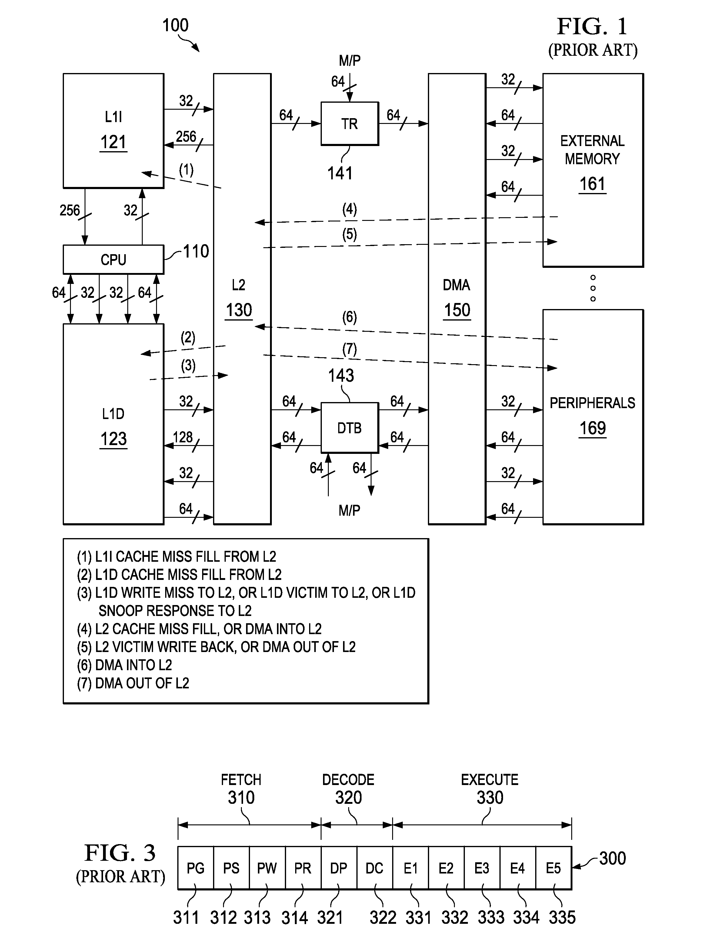
[0017]FIG. 1 illustrates the organization of a typical digital signal processor system 100 to which this invention is applicable (prior art). Digital signal processor system 100 includes central processing unit core 110. Central processing unit core 110 includes the data processing portion of digital signal processor system 100. Central processing unit core 110 could be constructed as known in the art and would typically include a register file, an integer arithmetic logic unit, an integer multiplier and program flow control units. An example of an appropriate central processing unit core is described below in conjunction with FIGS. 2 to 4.

[0018]Digital signal processor system 100 includes a number of cache memories. FIG. 1 illustrates a pair of first level caches. Level one instruction cache (L1I) 121 stores instructions used by central processing unit core 110. Central processing unit core 110 first attempts to access any instruction from level one instruction cache 121. Level one...


PUM


Abstract

This invention speeds operation for coherence writes to shared memory. This invention immediately commits to the memory endpoint coherence write data. Thus this data will be available earlier than if the memory controller stalled this write pending snoop responses. This invention computes write enable strobes for the coherence write data based upon the cache dirty tags. This invention initiates a snoop cycle based upon the address of the coherence write. The stored write enable strobes enable determination of which data to write to the endpoint memory upon a cached and dirty snoop response.

Description

CLAIM OF PRIORITY[0001]This application claims priority under 35 U.S.C. 119(e)(1) to U.S. Provisional Application No. 61 / 717,872 filed Oct. 24, 2012.TECHNICAL FIELD OF THE INVENTION[0002]The technical field of this invention is cache for digital data processors.BACKGROUND OF THE INVENTION[0003]This invention concerns multi-core data processing systems. It is typical in such multi-core systems for each core to have its own local cache memory and for all the cores to share a common higher level memory. This could be a memory on the same integrated circuit as the multiple cores (on chip) or an external memory (off chip). In such a multi-core data processing system more than one core may write to the same higher level memory. A multi-core shared memory controller must coordinate memory traffic between the multiple cores and the shared memory.[0004]This task includes contrary goals of maintaining coherence and suitable memory access latency. Each time one of the multiple cores updates a ...

Claims


Application Information

Patent Timeline
Patent Type & Authority Applications(United States)
IPC IPC(8): G06F12/08
CPCG06F12/0831G06F12/0828G06F13/1626G06F13/1663H04L63/0263G06F13/42G06F13/287G06F13/4022Y02D10/00G06F12/0815G06F21/79G06F21/78G06F12/1458G06F12/1491G06F13/1605G06F13/30G06F12/0835G06F12/1081G06F2212/621G06F12/0842G06F2212/1032G06F2212/283G06F2212/62
Inventor PIERSON, MATTHEW D.CHIRCA, KAIANDERSON, TIMOTHY D.
Owner TEXAS INSTR INC
Why Eureka
Try Eureka