Radiation induced diode structure

a diode and radiation-induced technology, applied in the field of semiconductor devices, can solve the problems of deteriorating the performance and the difficulty in obtaining long-term reliable operation of the bipolar junction transistor exposed to radiation

Active Publication Date: 2014-05-08
TEXAS INSTR INC
View PDF13 Cites 66 Cited by
  • Summary
  • Abstract
  • Description
  • Claims
  • Application Information

AI Technical Summary

Benefits of technology

[0004]The following presents a simplified summary in order to provide a basic understanding of one or more aspects of the invention. This summary is not an extensive overview of the invention, and is neither intended to identify key or critical elements of the invention, nor to delineate the scope thereof. Rather, the primary purpose of the summary is to present some concepts of the invention in a simplified form as a prelude to a more detailed description that is presented later.

Problems solved by technology

Trapped positive charge in a dielectric layer on a p-type semiconductor region may invert a surface of the p-type region adjacent to the trapped charge, forming a layer of electrons which may degrade performance of the bipolar junction transistor.
Obtaining long-term reliable operation of bipolar junction transistors exposed to radiation has been problematic.

Method used


Image

  • Radiation induced diode structure
  • Radiation induced diode structure
  • Radiation induced diode structure

Examples


Embodiment Construction

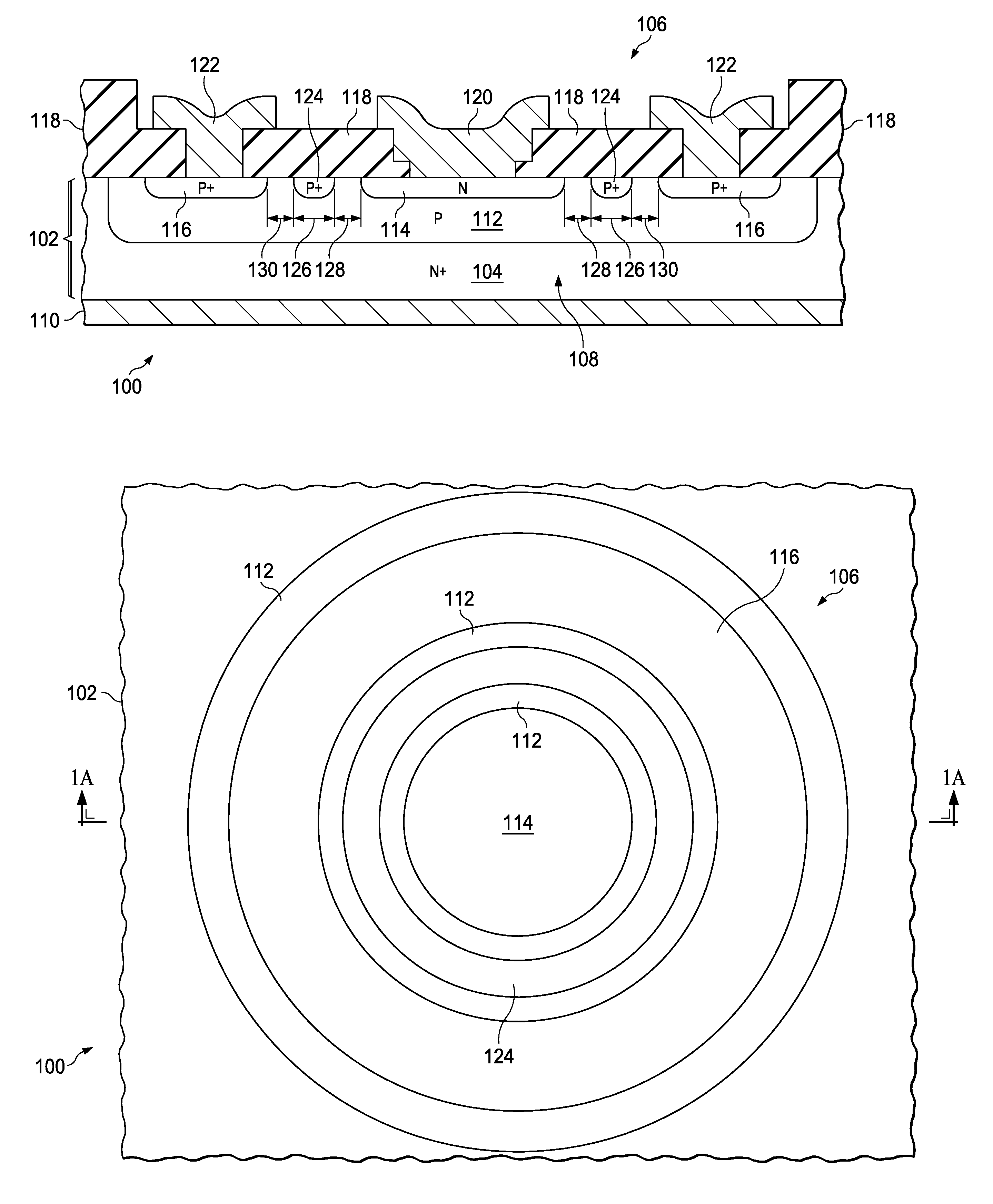
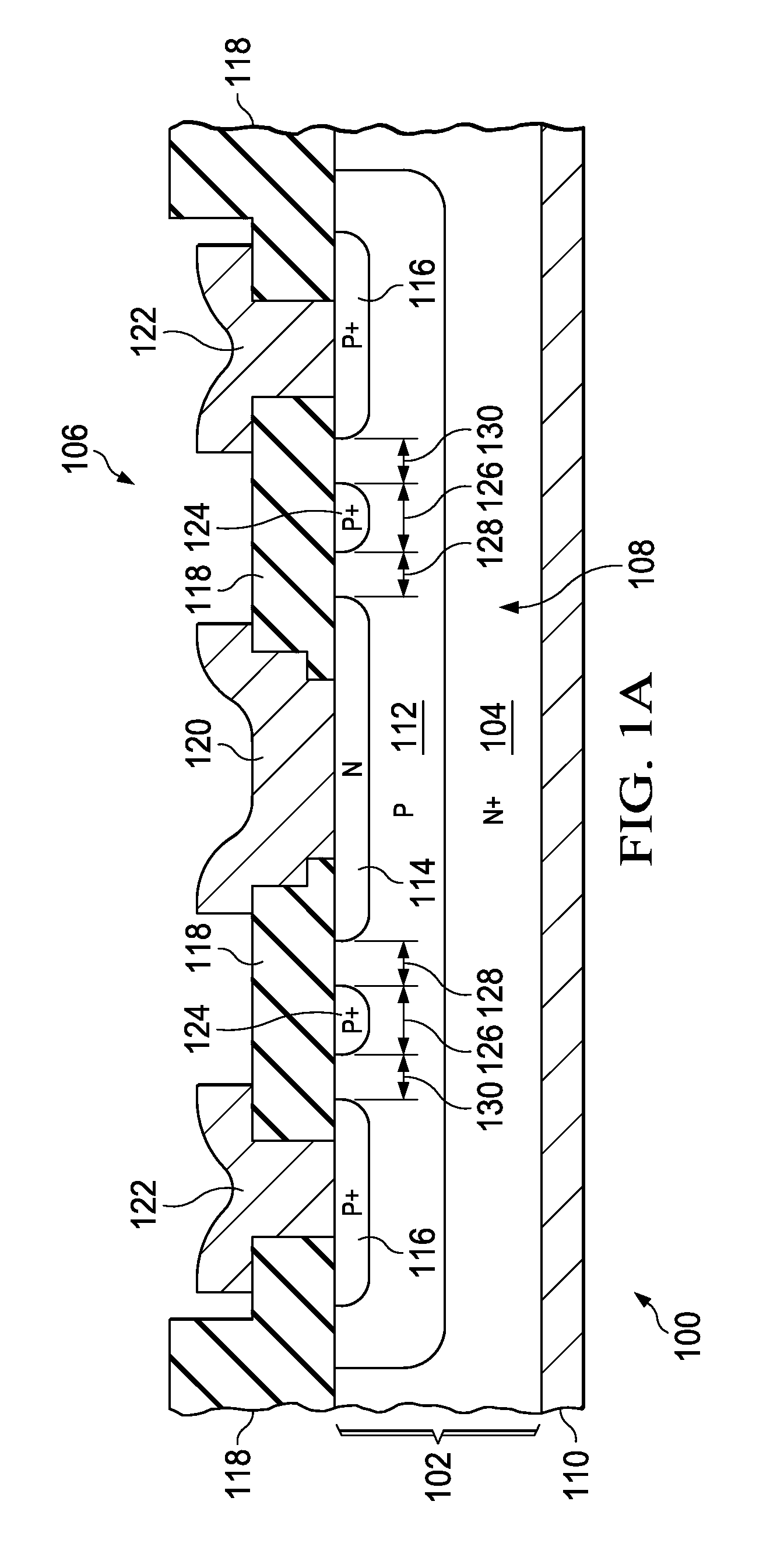
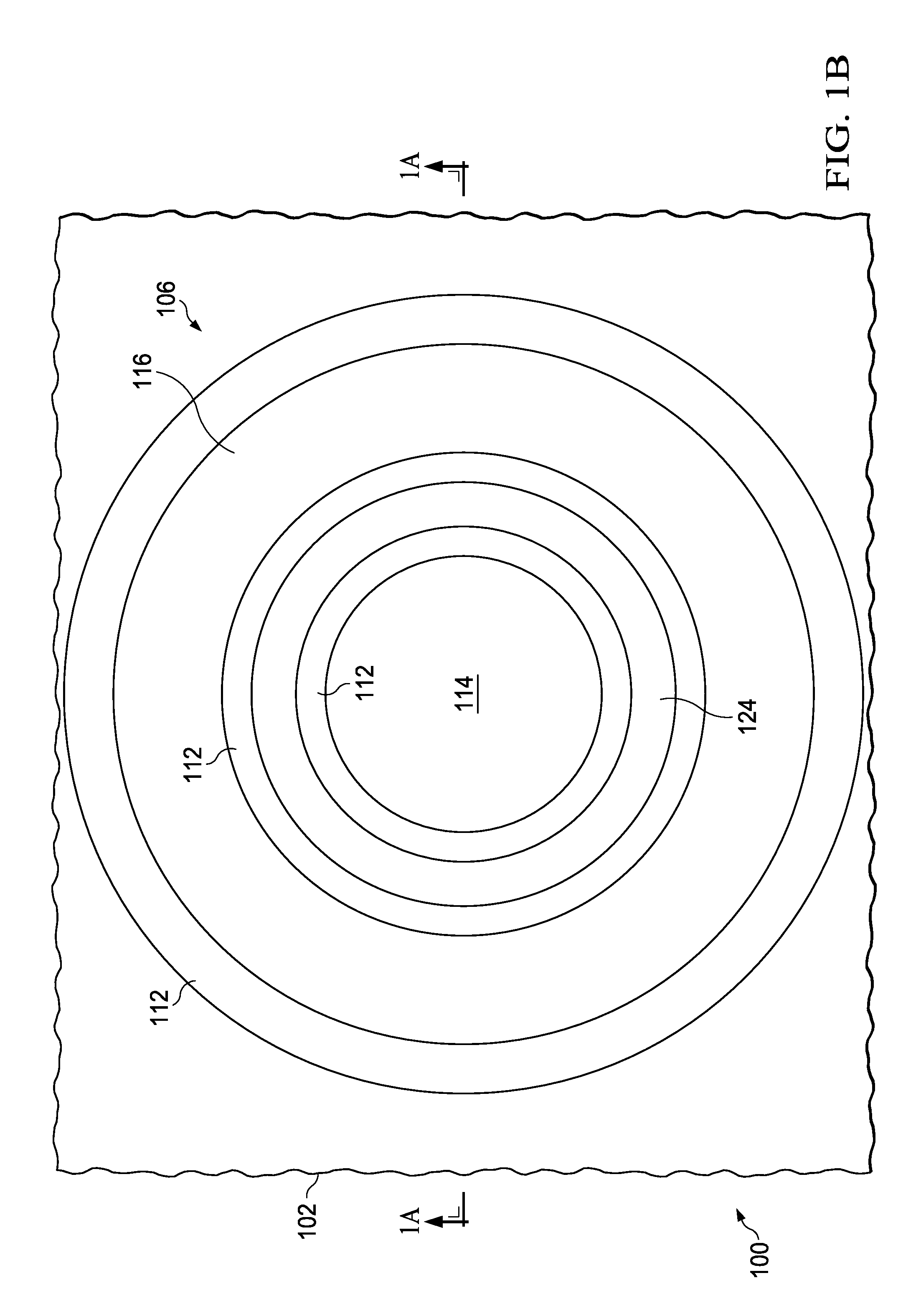
[0011]The present invention is described with reference to the attached figures. The figures are not drawn to scale and they are provided merely to illustrate the invention. Several aspects of the invention are described below with reference to example applications for illustration. It should be understood that numerous specific details, relationships, and methods are set forth to provide an understanding of the invention. One skilled in the relevant art, however, will readily recognize that the invention can be practiced without one or more of the specific details or with other methods. In other instances, well-known structures or operations are not shown in detail to avoid obscuring the invention. The present invention is not limited by the illustrated ordering of acts or events, as some acts may occur in different orders and / or concurrently with other acts or events. Furthermore, not all illustrated acts or events are required to implement a methodology in accordance with the pre...


PUM


Abstract

A semiconductor device containing an NPN bipolar junction transistor may be formed by forming a p-type radiation induced diode structure (RIDS) region in an intrinsic p-type base region of the NPN bipolar junction transistor at a boundary of the intrinsic p-type base region with a dielectric layer over a substrate of the semiconductor device, between an emitter of the NPN bipolar junction transistor and an extrinsic p-type base region of the NPN bipolar junction transistor. The p-type RIDS region has a doping density high enough to prevent inversion of a surface of the p-type RIDS region adjacent to the dielectric layer when trapped charge is accumulated in the dielectric layer, while the intrinsic p-type base region may invert from the trapped charge forming the radiation induced diode structure. The p-type RIDS region is separated from the emitter and from the extrinsic base region by portions of the intrinsic base region.

Description

CROSS-REFERENCE TO RELATED APPLICATIONS[0001]This application claims the benefit of priority under U.S.C. §119(e) of U.S. Provisional Application 61 / 723,025 (Texas Instruments docket number TI-73198PS) filed Nov. 6, 2012.FIELD OF THE INVENTION[0002]This invention relates to the field of semiconductor devices. More particularly, this invention relates to bipolar junction transistors in semiconductor devices.BACKGROUND OF THE INVENTION[0003]Semiconductor devices containing bipolar junction transistors which are exposed to radiation may accumulate trapped charge in dielectric layers. Trapped positive charge in a dielectric layer on a p-type semiconductor region may invert a surface of the p-type region adjacent to the trapped charge, forming a layer of electrons which may degrade performance of the bipolar junction transistor. Obtaining long-term reliable operation of bipolar junction transistors exposed to radiation has been problematic.SUMMARY OF THE INVENTION[0004]The following pres...

Claims


Application Information

Patent Timeline
Patent Type & Authority Applications(United States)
IPC IPC(8): H01L29/73H01L21/265H01L29/66
CPCH01L29/73H01L29/66234H01L21/265H01L29/66272H01L21/2652H01L29/0692H01L29/7322
Inventor SALZMAN, JAMES FREDROYBAL, RICHARD GUERRAKAHN, RANDOLPH WILLIAM
Owner TEXAS INSTR INC
Why Eureka
Try Eureka