

Substrate build up layer to achieve both finer design rule and better package coplanarity
- Summary
- Abstract
- Description
- Claims
- Application Information
AI Technical Summary
Benefits of technology
Problems solved by technology
Method used
Image

Examples
Embodiment Construction
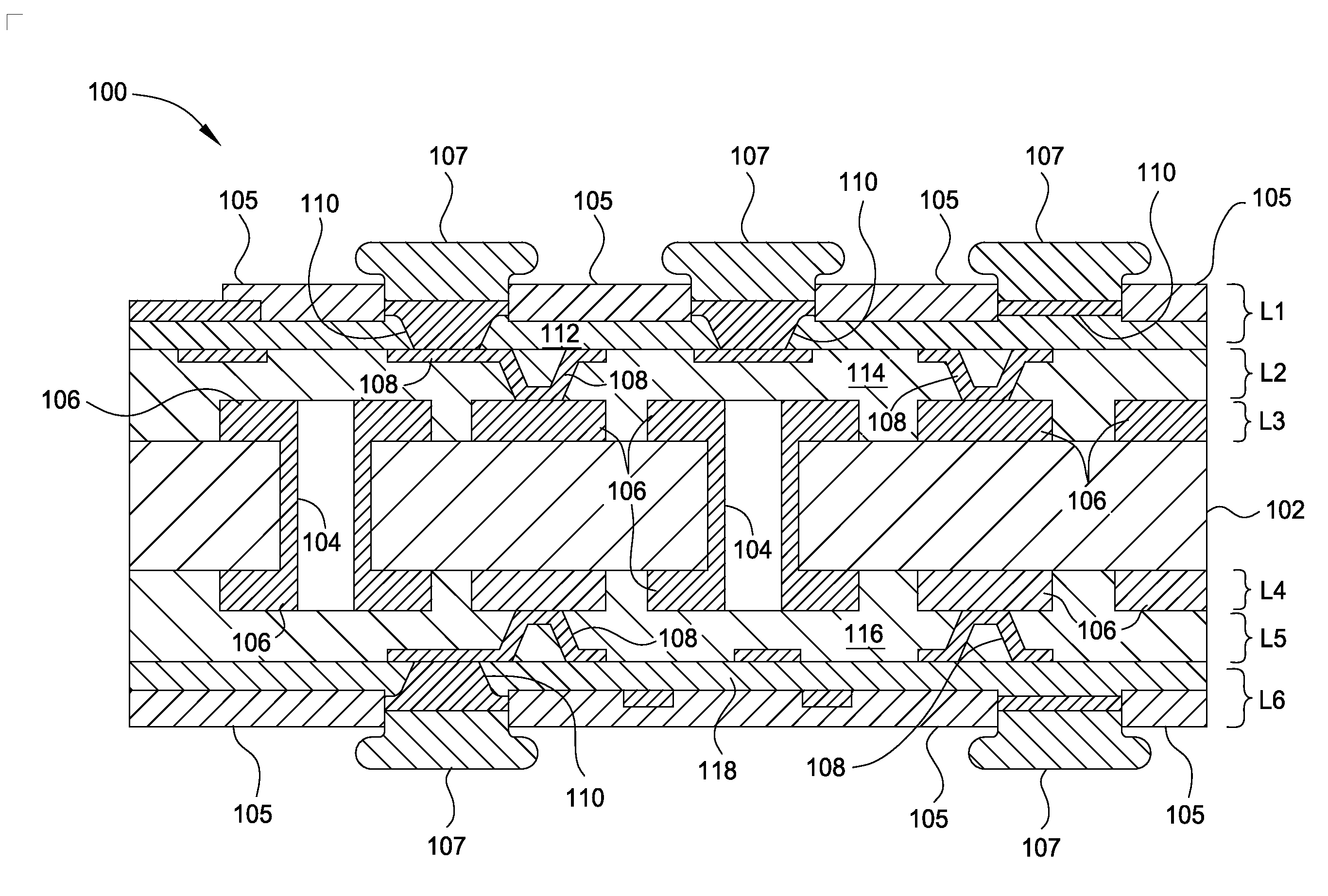
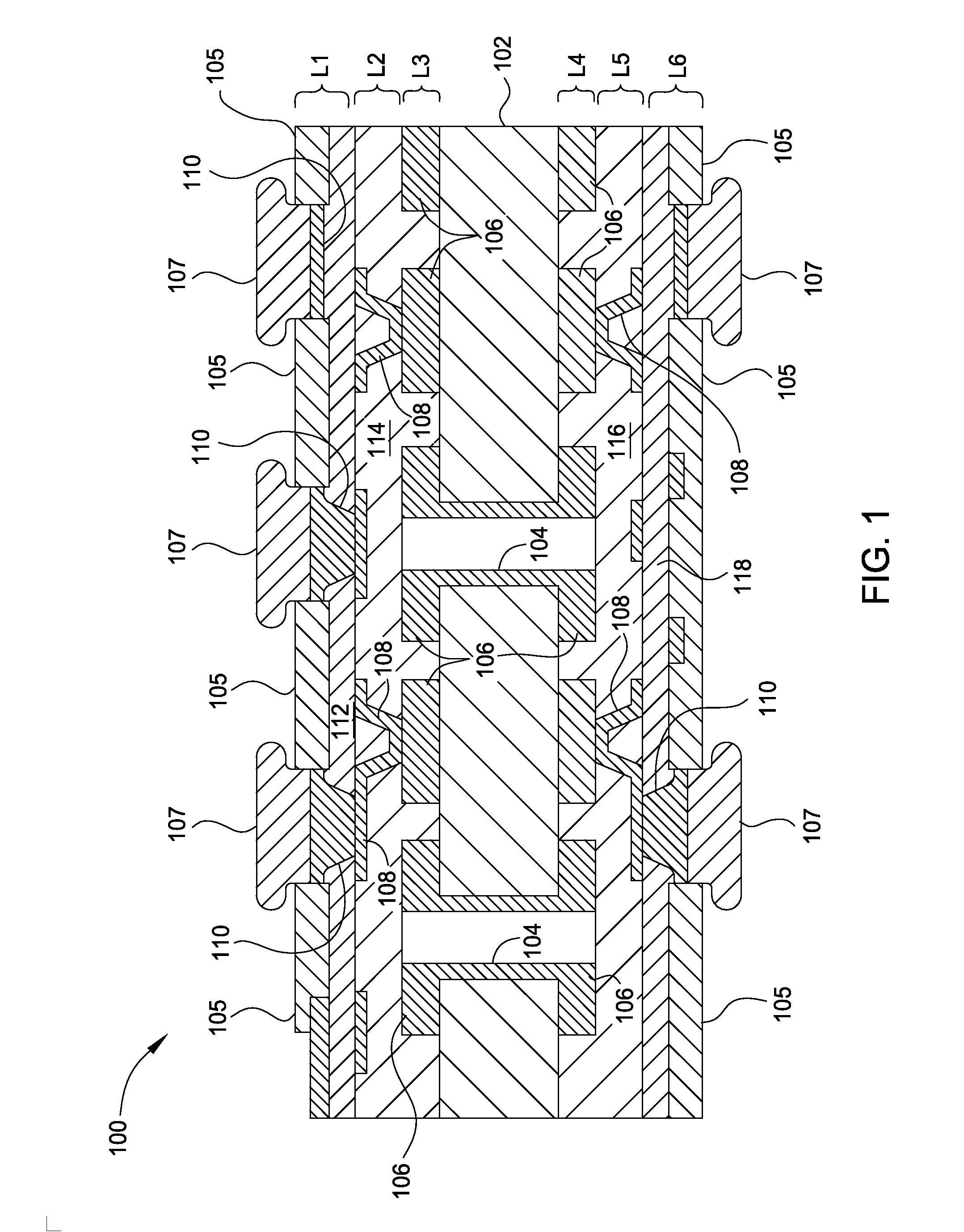
[0015]Embodiments of the invention generally relate to package substrates for integrated circuits. The package substrates each include a core having electrically conductive vias therethrough. Build-up layers formed from dielectric materials having different compositions are disposed around the core and include interconnects formed therein for facilitating electrical connections between integrated circuits coupled to the package substrate. The dielectric materials are selected to allow finer interconnect geometries where desired, and to increase the rigidity, and thus planarity, of the package substrate. The dielectric materials are selected based upon the desired stiffness or rigidity, the desired coefficients of thermal expansion, and the desired patterning capabilities. Exemplary dielectric materials include pre-impregnated composite fibers for increasing the rigidity of a package substrate, and Ajinomoto Build-up Film for allowing the formation finer interconnect geometries.
[0016...
PUM
 Abstract
Description
Claims
Application Information