Method For Testing Through-Silicon Vias At Wafer Sort Using Electron Beam Deflection

a technology of electron beam deflection and through-silicon vias, which is applied in the direction of measuring leads/probes, electric discharge tubes, instruments, etc., can solve the problems of difficult modification and challenge in the development of methodologies for testing tsvs, and achieve the effects of minimizing test time, maximizing beam direction tolerances, and minimizing test tim

Active Publication Date: 2014-05-08
ERICKSON BRIAN D
View PDF3 Cites 9 Cited by
  • Summary
  • Abstract
  • Description
  • Claims
  • Application Information

AI Technical Summary

Benefits of technology

[0011]According to other embodiments of the present invention, the TSV testing method involves directing the electron beam according to various scan patterns that either maximize beam direction tolerances, minimize test time, or are balanced to optimize both parameters. In a first beam directing embodiment, the electron beam is scanned in a raster-type pattern such that that it passes across the entire test wafer surface, thereby maximizing beam direction tolerances by eliminating the need to know where the TSVs are located. In a second beam directing embodiment, the electron beam is precisely positioned only each TSV based on stored targeting data, thereby minimizing test times by avoiding the generation of test data for inconsequential regions of the test wafer (i.e., regions that do not include a TSV). In a third beam directing embodiment, the electron beam is scanned in a limited raster-scan pattern over limited regions of the test wafer known to include one or more TSVs, and then moved from the first limited region to a second limited region. This third approach reduces test time by eliminating the need to scan regions known not to include TSVs, and also relaxes beam targeting tolerances by utilizing limited raster-type scanning patterns.

Problems solved by technology

Although TSVs facilitate superior 3D package arrangements, the development of methodologies for testing TSVs has proven to be a challenge.
The TSV production process leads to defects within the TSV which can include voids that produce improper (i.e., high impedance) connections to adjacent devices or interposer layers, thereby requiring that the integrity of each TSV also be tested during wafer sort.
Although it is possible to modify existing IC test equipment to configure two test probe arrays that respectively contact both sides of the wafer, this modification is problematic due to the complexity of simultaneously accessing a large number of contact pads disposed on both sides of a wafer.

Method used


Image

  • Method For Testing Through-Silicon Vias At Wafer Sort Using Electron Beam Deflection
  • Method For Testing Through-Silicon Vias At Wafer Sort Using Electron Beam Deflection
  • Method For Testing Through-Silicon Vias At Wafer Sort Using Electron Beam Deflection

Examples


Embodiment Construction

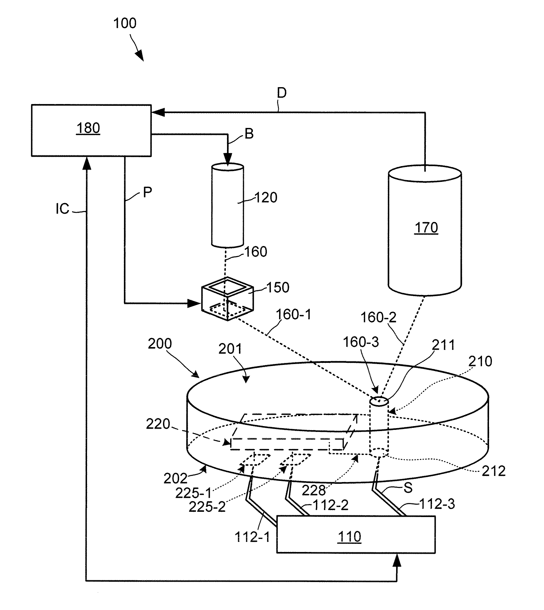
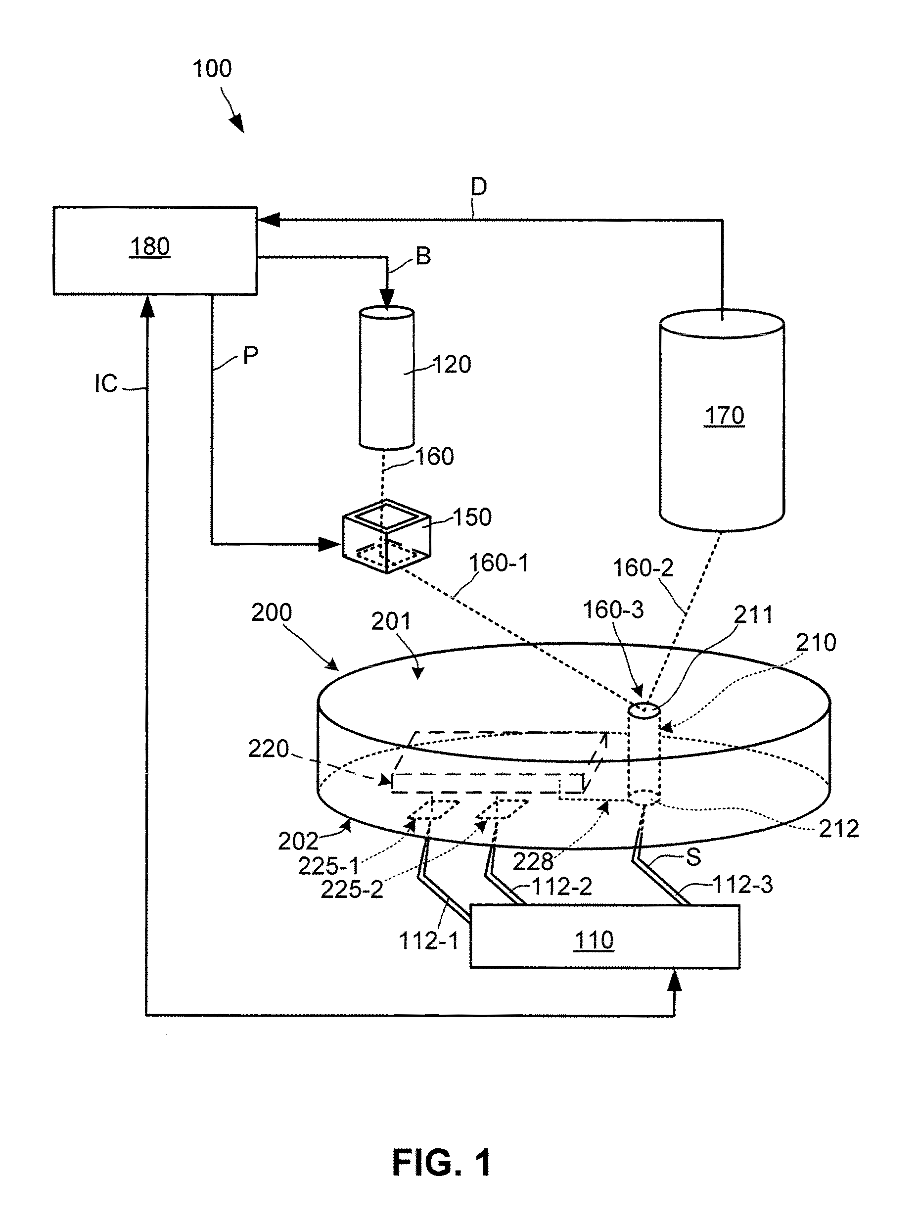
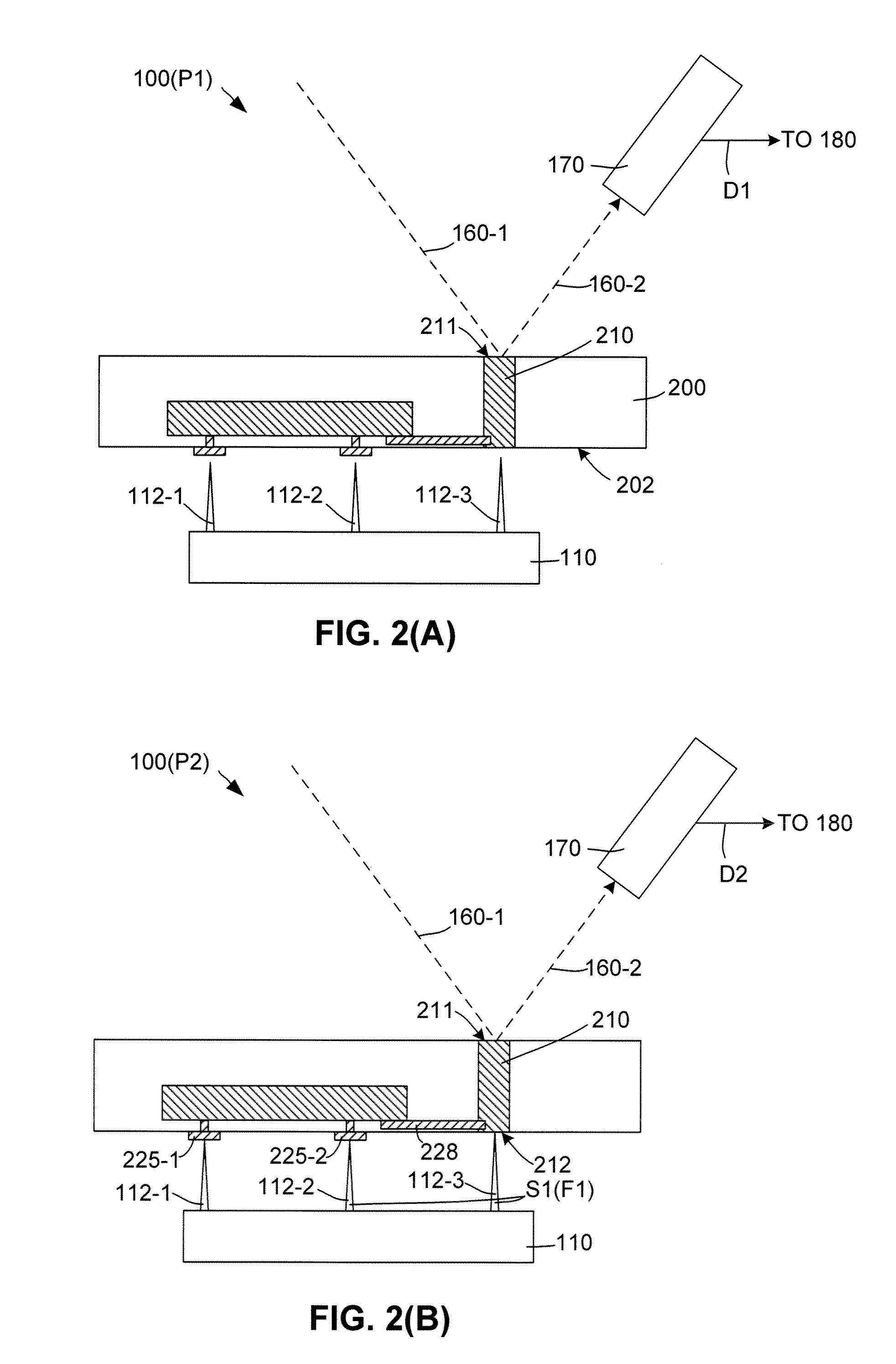
[0020]The present invention relates to an improvement in IC testing. The following description is presented to enable one of ordinary skill in the art to make and use the invention as provided in the context of a particular application and its requirements. As used herein, directional terms such as “upper” and “lower” are intended to provide relative positions for purposes of description, and are not intended to designate an absolute frame of reference. The terms “coupled” and “connected”, which are utilized herein, are defined as follows. The term “connected” is used to describe a direct connection between two circuit elements, for example, by way of a metal line formed in accordance with normal integrated circuit fabrication techniques. In contrast, the term “coupled” is used to describe either a direct connection or an indirect connection between two circuit elements. For example, two coupled elements may be directly connected by way of a metal line, or indirectly connected by wa...


PUM


Abstract

Through-silicon vias (TSVs) are tested using a modified integrated circuit test probe array, an electron beam generation device, a beam direction control device and an electron beam detection device. The TSV extends through a silicon substrate with end portions exposed or accessible by contacts disposed on opposing upper and lower surfaces of the substrate. The test probe array includes a test probe that accesses the lower TSV end portion and applies an AC test signal. An electron beam is directed by the beam direction control device onto the upper substrate surface such that a beam portion reflected from the upper TSV end portion is captured by the electron beam detection device. Reflected beam data is then analyzed to verify the TSV is properly formed. Various scan patterns, different test signal frequencies and an optional resistive coating are used to enhance the TSV testing process.

Description

RELATED APPLICATIONS[0001]This application claims priority to U.S. Provisional Patent Application 61 / 722,738, entitled “METHOD AND STRUCTURE FOR PROVIDING REDUCED CONTACT TESTING AT WAFER SORT USING ELECTRON BEAM DEFLECTION” filed Nov. 5, 2012.FIELD OF THE INVENTION[0002]The present invention related to integrated circuits, and more particularly to methods for testing integrated circuit wafers including to through-silicon vias (TSVs) assure proper operation prior to assembly.BACKGROUND OF THE INVENTION[0003]FIG. 7 shows a simplified semiconductor device disposed in a three-dimensional (3D) package arrangement including two silicon chips 10-1 and 10-2 that are stacked vertically and separated by an insulating layer 13. Silicon chip 10-1 and 10-2 respectively include integrated circuits (ICs) 20-1 and 20-2 fabricated thereon using conventional (e.g., CMOS) fabrication processes, with IC 20-1 being connected by conventional metal wiring structures to contact pads 17 and to a conductor ...

Claims


Application Information

Patent Timeline
Patent Type & Authority Applications(United States)
IPC IPC(8): G01R1/07G01R31/50
CPCG01R1/07G01R31/307G01R31/50
Inventor ERICKSON, BRIAN D.
Owner ERICKSON BRIAN D
Why Eureka
Try Eureka