Method for manufacturing piezoelectric device

a piezoelectric device and manufacturing method technology, applied in the direction of electrical transducers, transducer types, electric/electrostrictive transducers, etc., can solve the problems of damage to piezoelectric thin films, and the effect of preventing the degradation of piezoelectricity of piezoelectric thin films

Active Publication Date: 2014-05-15
MURATA MFG CO LTD
View PDF3 Cites 76 Cited by
  • Summary
  • Abstract
  • Description
  • Claims
  • Application Information

AI Technical Summary

Benefits of technology

[0035]One of the advantageous effects of various preferred embodiments of the present invention is to prevent the degradation of the piezoelectricity of the piezoelectric thin film and damage to the piezoelectric thin film.
[0036]T...

Problems solved by technology

This means that piezoelectric thin film devices produced by the manufacturing method according to Japanese Unexamined Patent Application Publication No. 2002-534886 are disadvantageous because of degraded piezoelectricity.
This is a fatal problem for the device characteristics of high-frequency filters in particular because in devices of th...

Method used


Image

  • Method for manufacturing piezoelectric device
  • Method for manufacturing piezoelectric device
  • Method for manufacturing piezoelectric device

Examples


embodiment 1

[0060]The following describes the manufacturing method of piezoelectric devices according to Preferred Embodiment 1 of the present invention with reference to drawings. In the following description, a method for manufacturing surface acoustic wave devices is detailed as an illustrative manufacturing method of piezoelectric devices.

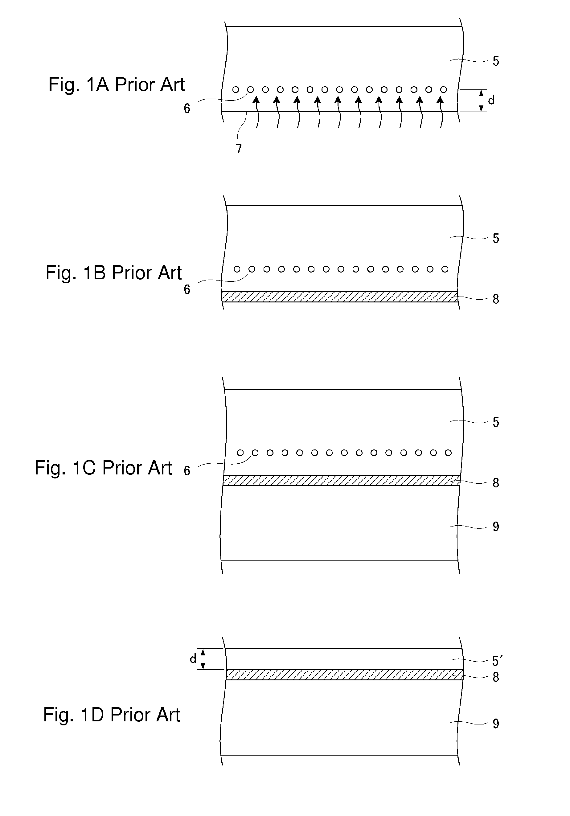
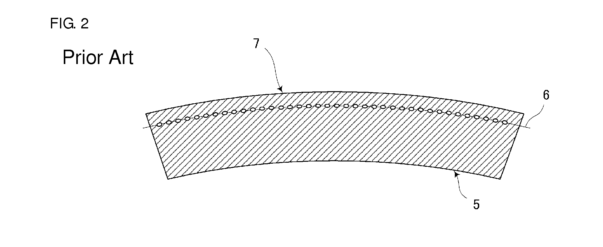
[0061]FIG. 3 is a flowchart illustrating the manufacturing method of piezoelectric devices according to Preferred Embodiment 1. FIGS. 4A and 4B and FIGS. 6A to 8B show schematic cross-sectional diagrams illustrating the manufacturing steps of piezoelectric devices according to Preferred Embodiment 1. FIG. 5A is a schematic diagram illustrating a warped piezoelectric single crystal substrate after an ion implantation step, and FIG. 5B is a schematic diagram illustrating the piezoelectric single crystal substrate relieved from its warped state by the action a compressive stress film.

[0062]The first step is to prepare a piezoelectric single crystal substrate ...

embodiment 2

[0091]The following describes the manufacturing method of piezoelectric devices according to Preferred Embodiment 2 of the present invention with reference to FIGS. 9 to 12B. In the following description, a method for manufacturing surface acoustic wave devices is detailed as an illustrative manufacturing method of piezoelectric devices.

[0092]FIG. 9 is a flowchart illustrating the manufacturing method of piezoelectric devices according to Preferred Embodiment 2. FIGS. 10 and 11 show schematic cross-sectional diagrams illustrating the manufacturing steps of piezoelectric devices presented in FIG. 9. Preferred Embodiment 2 is different from Preferred Embodiment 1 in that it includes a provisional support formation step; the procedures up to the compressive stress film formation step are the same.

[0093]After the compressive stress film formation step (S202 in FIGS. 9 and 10), an etching substrate layer formation step is carried out to place an etching substrate layer 3 on the surface o...

embodiment 3

[0107]The following describes the manufacturing method of piezoelectric devices according to Preferred Embodiment 3 with reference to drawings. In the following description, a method for manufacturing surface acoustic wave devices is detailed as an illustrative manufacturing method of piezoelectric devices.

[0108]FIG. 13 is a flowchart illustrating the manufacturing method of piezoelectric devices according to Preferred Embodiment 3. FIG. 14A is a schematic diagram illustrating a piezoelectric single crystal substrate warped by the action of a compressive stress film. FIG. 14B is a schematic diagram illustrating ions implanted into the piezoelectric single crystal substrate warped by the action of a compressive stress film; the ions are implanted from the front of the piezoelectric substrate. FIG. 14C is a schematic diagram illustrating the piezoelectric single crystal substrate after the ion implantation step; the piezoelectric substrate is relieved from its warped state.

[0109]The m...


PUM

PropertyMeasurementUnit
Temperatureaaaaaaaaaa
Thicknessaaaaaaaaaa
Dielectric polarization enthalpyaaaaaaaaaa

Abstract

In a method of manufacturing a piezoelectric device, a compressive stress film is formed on a back surface of a piezoelectric single crystal substrate opposite to a surface on an ion-implanted side. The compressive stress film compresses the surface on the ion-implanted side of the piezoelectric single crystal substrate. The compressive stress produced by the compressive stress film is applied to half of the piezoelectric single crystal substrate on the ion-implanted side with respect to the center line of the thickness of the piezoelectric single crystal substrate to prevent the piezoelectric single crystal substrate from warping. A supporting substrate is then bonded to the surface of a bonding film on the flat piezoelectric single crystal substrate. The joined body of the piezoelectric single crystal substrate and the supporting substrate is then heated to initiate isolation at the ion-implanted portion as the isolation plane.

Description

BACKGROUND OF THE INVENTION[0001]1. Field of the Invention[0002]The present invention relates to a method for manufacturing a piezoelectric device that uses a thin film made of a piezoelectric single crystal material.[0003]2. Description of the Related Art[0004]Many kinds of piezoelectric devices that utilize a piezoelectric thin film, i.e., thin-film piezoelectric devices, are now under development. There are many ways to produce a piezoelectric thin film for the fabrication of thin-film piezoelectric devices. For example, Japanese Unexamined Patent Application Publication No. 2002-534886 proposes a method for manufacturing a piezoelectric device in which a piezoelectric thin film is formed by isolation from a piezoelectric substrate at an ion-implanted layer as the isolation plane.[0005]The following describes this manufacturing method of a piezoelectric device, which includes forming a piezoelectric thin film by isolation from a piezoelectric substrate at an ion-implanted layer a...

Claims


Application Information

Patent Timeline
IPC IPC(8): H03H3/02H01L41/312H01L41/335
CPCH03H3/02H03H3/08H03H9/02574H03H9/059H03H9/173H01L2224/11Y10T29/42Y10T29/49005Y10T29/49124H10N30/072H03H2003/023H03H2003/025H03H9/02543H03H9/174H01L21/02697H10N30/092
Inventor IWAMOTO, TAKASHI
Owner MURATA MFG CO LTD
Why Eureka
Try Eureka