Method of detecting wire bonding failures

a technology of failure detection and wire bonding, which is applied in the direction of solid-state devices, manufacturing tools, and soldering apparatus, etc., can solve the problems of non-stick-on-lead (‘nsol’) bonding failur

Active Publication Date: 2014-05-15
ASMPT SINGAPORE PTE LTD
View PDF3 Cites 15 Cited by
  • Summary
  • Abstract
  • Description
  • Claims
  • Application Information

AI Technical Summary

Problems solved by technology

A non-stick-on-lead (‘NSOL’) bonding failure occurs if the wire is not properly bonded to the substrate via the wedge bond.
However, the aforesaid method of detecting NSOL bonding failure is applicable only to conductive semiconductor dies and not to non-conductive semiconductor dies.

Method used


Image

  • Method of detecting wire bonding failures
  • Method of detecting wire bonding failures
  • Method of detecting wire bonding failures

Examples


Embodiment Construction

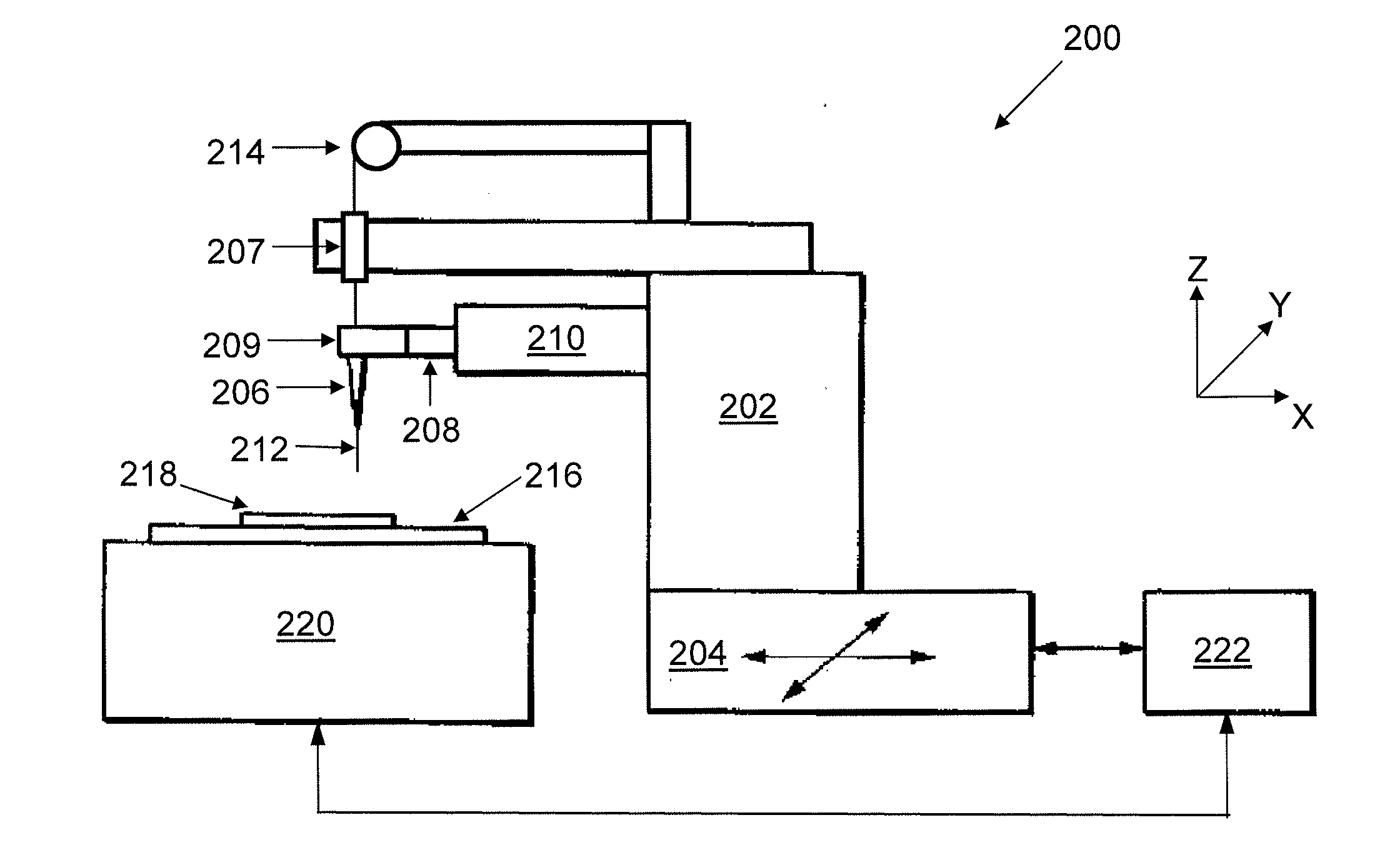
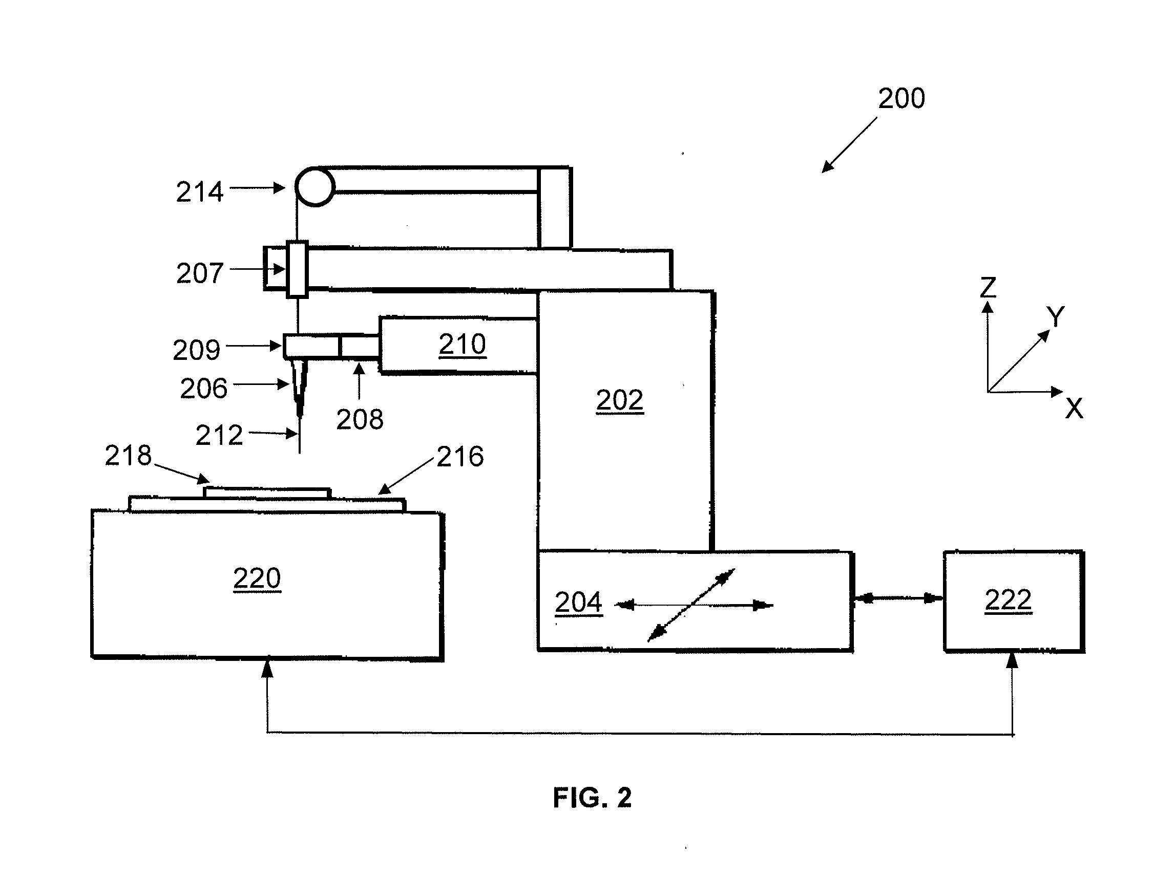
[0017]FIG. 2 shows a wire bonder 200 that is capable of detecting NSOL bonding failure according to a preferred embodiment of the invention. The wire bonder 200 comprises a bond head 202 connected to an XY table 204, which is in turn connected to a control device (shown as a personal computer 222) that controls the various parts of the wire bonder 200 during operation. A bonding tool (shown as a capillary 206), together with an ultrasonic transducer 208 and an ultrasonic horn 209, is connected to the bond head 202 via a bond arm 210 that extends from the bond head 202. A bonding wire 212 (e.g. Copper or Gold wire) from a wire spool 214 is introduced through a wire clamp 207 and the capillary 206. The wire bonder 200 also comprises a top plate 216 for supporting a substrate (shown as a lead frame 218) to which semiconductor dies (e.g. LED dies) are bonded. The top plate 216 is supported on a fixed table 220, which is also connected to the personal computer 222. During wire bonding, t...


PUM

PropertyMeasurementUnit
tail lengthaaaaaaaaaa
lengthsaaaaaaaaaa
electrically-conductiveaaaaaaaaaa

Abstract

Disclosed is a method of detecting a bonding failure of a wire bonder, which comprises a bonding tool operative to form an electrical connection between a semiconductor die and a substrate using a bonding wire. The method comprises the steps of: forming a first wire bond on a first surface located on the semiconductor die using the bonding tool and the bonding wire; forming a second wire bond on a second surface located on the substrate using the bonding tool and the bonding wire such that a wire loop connects the first and second wire bonds, wherein the first surface is not electrically-conductive; moving the bonding tool in a direction away from the second wire bond to break the bonding wire from the second wire bond; detecting whether the second wire bond remains bonded to the substrate; and determining an occurrence of the bonding failure if the second wire bond is no longer bonded to the substrate.

Description

FIELD OF THIS INVENTION[0001]This invention relates to a method of detecting wire bonding failures during semiconductor device fabrication.BACKGROUND OF THE INVENTION[0002]Semiconductor device fabrication involves many processes including wire bonding processes, in which electrical connections are formed between a semiconductor die (e.g. an integrated circuit die) and a substrate (e.g. a lead frame) to which the semiconductor die is bonded. In conventional wire bonding processes, a free air ball is first formed at one end of a wire before bonding the free air ball to the semiconductor die via ball bonding. Another wire bond (e.g. a wedge bond) is then formed between the wire and the substrate (e.g. a lead frame) to form an electrical connection between the semiconductor die and the substrate. Thereafter, the wire is clamped before being pulled in a direction away from substrate to detach the wire at the location of the wedge bond.[0003]A non-stick-on-lead (‘NSOL’) bonding failure oc...

Claims


Application Information

Patent Timeline
Patent Type & Authority Applications(United States)
IPC IPC(8): B23K3/08
CPCB23K3/08H01L24/78H01L24/85H01L2224/859H01L2224/78353H01L24/45H01L24/48H01L2224/45144H01L2224/45147H01L2224/48091H01L2224/48247H01L2224/48465H01L2224/78301H01L2224/78601H01L2224/78801H01L2224/85205H01L2924/12041H01L2224/7892H01L2924/00014H01L2924/00
Inventor LIU, WEIZHANG, QIANLEE, JOON HOKIM, JUNG MIN
Owner ASMPT SINGAPORE PTE LTD
Why Eureka
Try Eureka