Eureka AIR delivers breakthrough ideas for toughest innovation challenges, trusted by R&D personnel around the world.

Lighting apparatus for measuring electronic material-processed part and test apparatus using the same

Inactive Publication Date: 2014-05-15
ADVANCED TECH
View PDF0 Cites 10 Cited by
  • Summary
  • Abstract
  • Description
  • Claims
  • Application Information

AI Technical Summary

Benefits of technology

The present invention provides a lighting apparatus that can clearly image a processed part of a variety of electronic parts or materials, allowing for easy detection of defects such as scrapes, cracks, chipps, and sawing line defects. This apparatus can be used in conjunction with a photographing apparatus and provides a reliable and precise means of testing the sawing line of a wafer.

Problems solved by technology

In the laser drilling process, there is a problem in that melt or evaporated silicon particles are adhered to a surface of a substrate.
In the industry field, however, the mechanical cutting method is being used a lot owing to a price problem.
Most of conventional methods used to obtain a precise image are problematic in that illumination thereof is weak.
However, to illuminate all the portions of a sawing line uniformly is difficult.
Although a wafer is precisely cut, environmental factors and mechanical defects appear when an image of a cut sawing line is enlarged with ultra-high precision.
This can deteriorate the quality of the chips 20 and can also become a cause of a defect.
This is a diamond cutting defect.
Furthermore, the above problem also has an error in that an image of a cut product cannot be precisely obtained.
In particular, in the case of coaxial illumination, this phenomenon becomes severe.
This results in a problem in a precise test because light is not emitted or a shadow area that derives diffused reflection is generated.
As a result, there is a disadvantage in that a precise test becomes difficult because a precise image cannot be obtained.

Method used


Image

  • Lighting apparatus for measuring electronic material-processed part and test apparatus using the same
  • Lighting apparatus for measuring electronic material-processed part and test apparatus using the same
  • Lighting apparatus for measuring electronic material-processed part and test apparatus using the same

Examples


Embodiment Construction

[0040]Lighting apparatus for measuring an electronic material-processed part and a test apparatus using the same in accordance with some exemplary embodiments of the present invention are described in detail below with reference to the accompanying drawings.

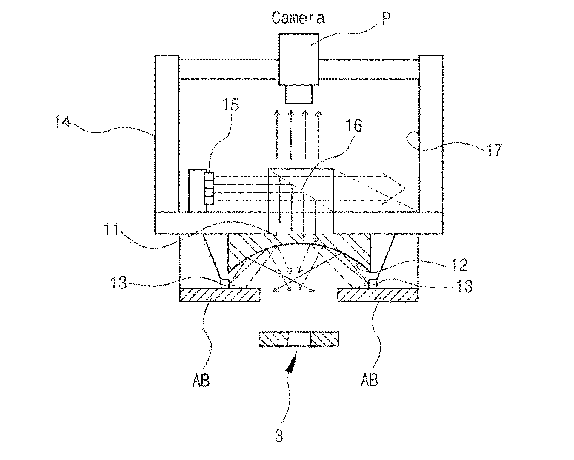
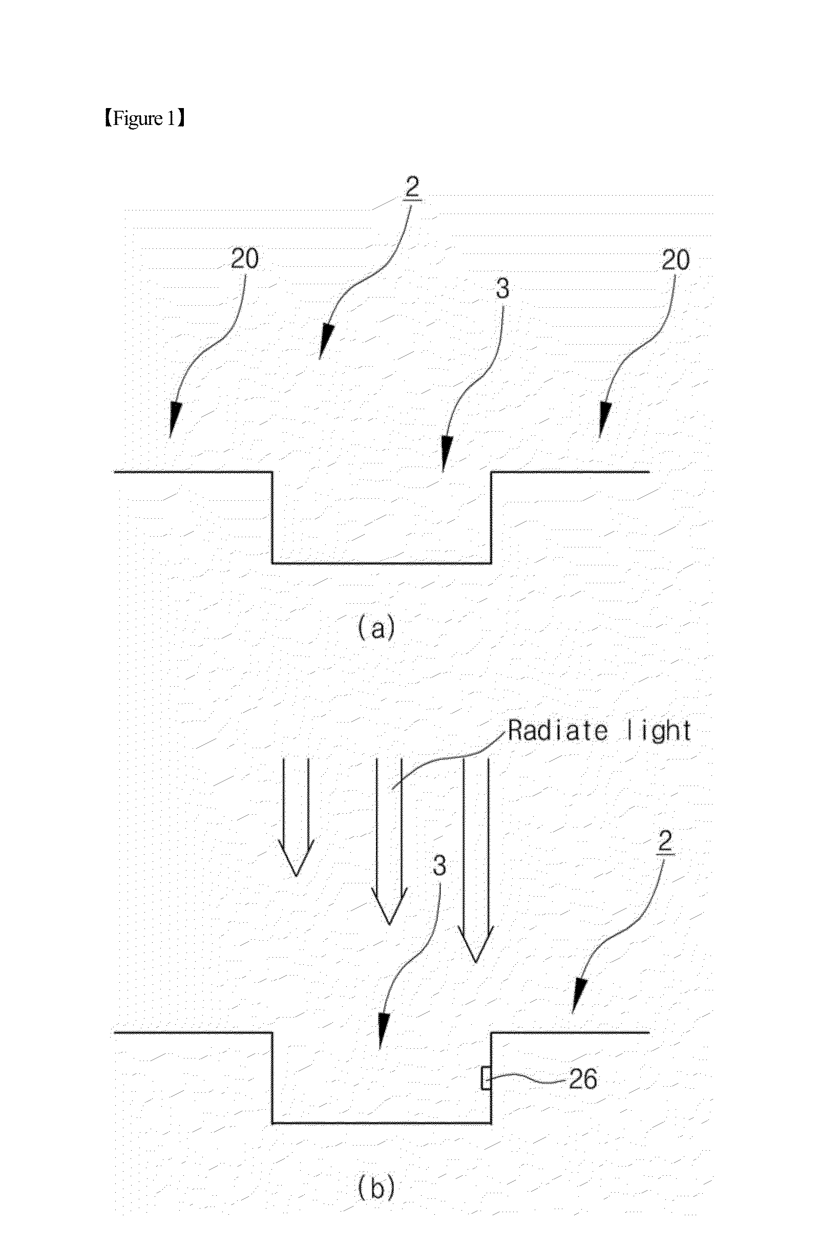
[0041]The lighting apparatus for measuring an electronic material-processed part in accordance with the present invention is configured to have a dome form in such a way as to be placed over the subject of measurement and configured to include a light inflow window 11 formed at the central part of the highest end of the lighting apparatus so that coaxial illumination can enter or exit from the light inflow window 11, a dome reflection plate 12 configured to reflect incident light in all directions, a plurality of dome illumination lamps 13 disposed at lower edge portions of the dome reflection plate 12 and configured to illuminate the inside of the dome, and a camera 20 disposed right over the light inflow window 11 for the coaxi...


PUM


Abstract

The present invention relates to lighting apparatus for measuring an electronic material-processed part and the test apparatus using the same. The lighting apparatus includes a dome reflection plate 12 disposed over the subject of measurement and configured to have a dome form, have a light inflow window 11 through which coaxial illumination enters or exits formed at a central part of a highest end of the dome reflection plate 12, and have incident light reflected in all directions within the dome; a plurality of dome illumination lamps 13 disposed at lower edge portions of the dome reflection plate 12 and configured to illuminate the inside of the dome; and a camera 20 disposed right over the light inflow window 11 for the coaxial illumination of the dome reflection plate 12. The lighting apparatus illuminates a processing part, that is, the subject of measurement.

Description

CROSS REFERENCE TO RELATED APPLICATION[0001]This application claims the benefit of Korean Patent Application No. 10-2012-0127934, filed Nov. 13, 2012, which is hereby incorporated by reference in its entirety into this application.BACKGROUND OF THE INVENTION[0002]1. Technical Field[0003]The present invention relates to lighting apparatus for measuring an electronic material-processed part and a test apparatus using the same and, more particularly, to lighting apparatus for a test apparatus for testing the degree of precision of a processed part and whether there is a defect or not when producing a variety of electronic materials or parts. In particular, a substantial example of the present invention relates to lighting apparatus and a test apparatus using the same for checking a minute scar in a processing part (e.g., a sawing line) that is formed by a diamond sawing process for cutting a semiconductor wafer.[0004]2. Description of the Related Art[0005]A substrate cutting and separa...

Claims


Application Information

Patent Timeline
IPC IPC(8): F21V7/00H04N7/18
CPCH04N7/18F21V7/00G01B2210/56G01N21/8806G01N21/9501G01N21/956H01L22/12G01B11/00G01N21/88
Inventor YOON, DOO HYUNAN, DOO BAECKKIM, JIN YOUNG
Owner ADVANCED TECH
Why Eureka
Eureka Blog
Learn More