
Organic light-emitting display device and method of manufacturing the same

Inactive Publication Date: 2014-05-22
SAMSUNG DISPLAY CO LTD
View PDF18 Cites 7 Cited by
  • Summary
  • Abstract
  • Description
  • Claims
  • Application Information

AI Technical Summary

Benefits of technology

The present invention provides an organic light emitting display device and a method of manufacturing it that reduces voltage drop at the counter electrode. This is achieved by coupling an auxiliary electrode to the counter electrode through a planarization layer. This improves the reliability of the organic light emitting display device.

Problems solved by technology

However, since the thickness of a metal film is inversely proportional to the resistance of the metal film, a voltage drop frequently occurs due to the high resistance of the counter electrode.
As a result, it may be difficult to form clear images and the reliability of the organic light emitting display having this structure is low.

Method used


Image

  • Organic light-emitting display device and method of manufacturing the same
  • Organic light-emitting display device and method of manufacturing the same
  • Organic light-emitting display device and method of manufacturing the same

Examples


Embodiment Construction

[0023]As used herein, the term “and / or” includes any and all combinations of one or more of the associated listed items.

[0024]Hereinafter, exemplary embodiments of the present invention will be described in detail with reference to the attached drawings.

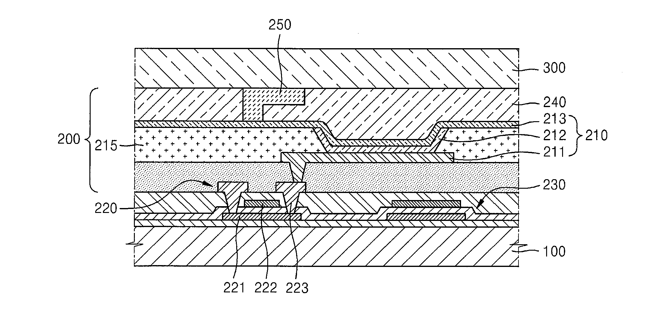
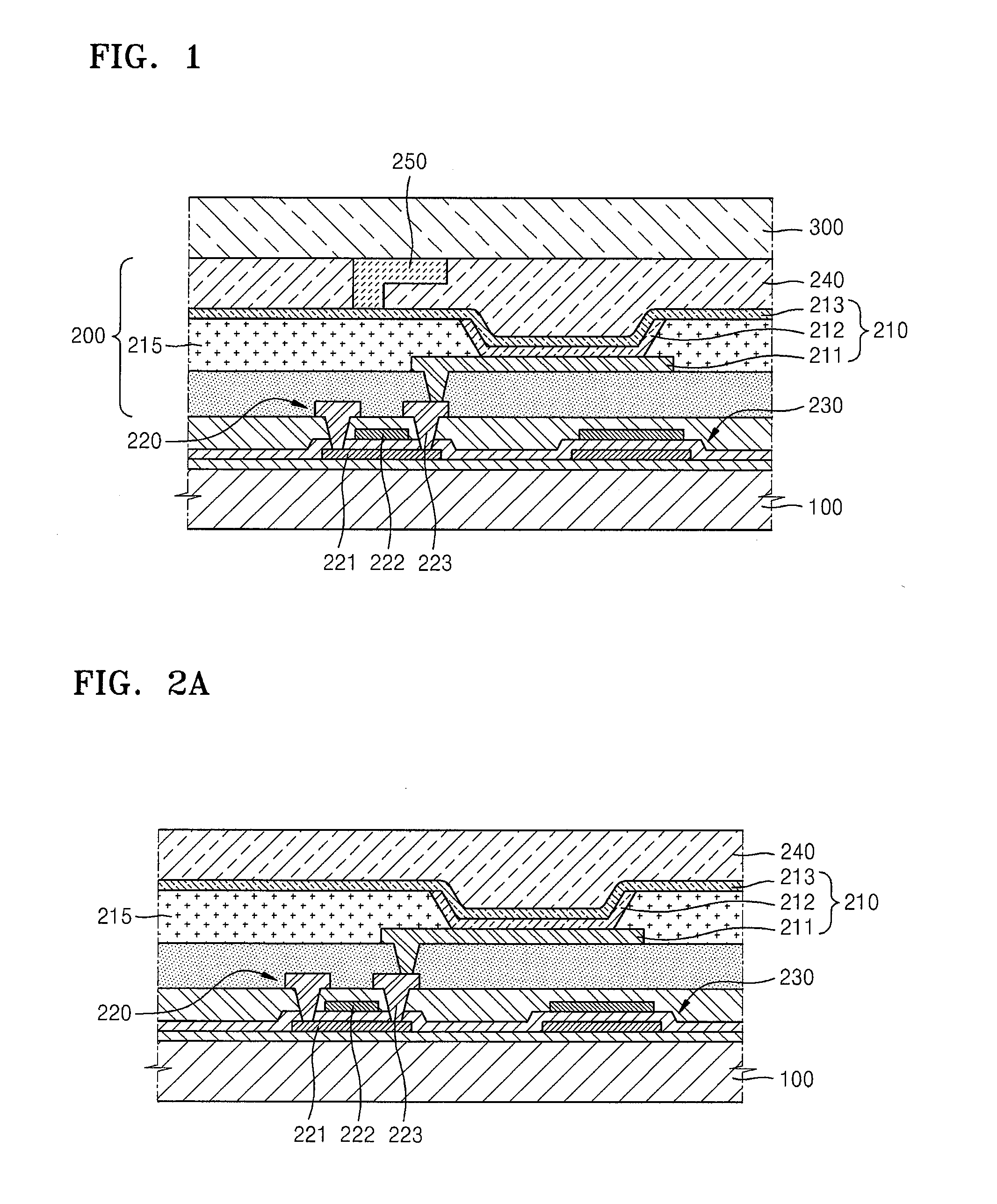
[0025]FIG. 1 is a cross-sectional view illustrating an organic light emitting display device according to an embodiment of the present invention. As illustrated in FIG. 1, the organic light emitting display device according to the present embodiment includes a base substrate 100, a display unit 200 formed thereon, and an encapsulation layer 300 covering the display unit 200.

[0026]The display unit 200 includes a thin-film transistor (TFT) 220, a capacitor 230, and an organic light emitting device 210. FIG. 1 shows a sub-pixel of the display unit 200 of the organic light emitting display device, and a plurality of such sub-pixels may be arranged in rows and columns on the base substrate 100.

[0027]The TFT 220 includes an active layer 22...


PUM


Abstract

An organic light emitting display device including a sub-pixel including a pixel electrode, a counter electrode, and a light emitting layer between the pixel electrode and the counter electrode, a planarization layer covering the counter electrode, and an auxiliary electrode in the planarization layer and coupled to the counter electrode.

Description

CROSS-REFERENCE TO RELATED PATENT APPLICATION[0001]This application claims priority to and the benefit of Korean Patent Application No. 10-2012-0131117, filed on Nov. 19, 2012 in the Korean Intellectual Property Office, the disclosure of which is incorporated herein in its entirety by reference.BACKGROUND[0002]1. Field[0003]Embodiments of the present invention relate to an organic light emitting display device and a method of manufacturing the same, and more particularly, to an organic light emitting display device having a structure for reducing or preventing a voltage drop at a counter electrode and a method of manufacturing the organic light emitting display device.[0004]2. Description of the Related Art[0005]Generally, an organic light emitting display device has a stacked structure in which a light emitting layer is located between a pixel electrode, which is an anode, and a counter electrode, which is a cathode. Colors are formed when holes and electrons respectively injected ...

Claims


Application Information

Patent Timeline
IPC IPC(8): H01L51/52
CPCH10K59/80522H10K59/1315H10K50/824
Inventor CHUNG, IN-YOUNG
Owner SAMSUNG DISPLAY CO LTD
Learn More