Package carrier

a technology of packaging and carrier, applied in the direction of circuit thermal arrangement, printed circuit aspects, solid-state devices, etc., can solve the problems of poor heat dissipation, reduced layout space, increased carrier area, etc., to improve the use efficiency and lifespan of effectively dissipate the heat generated by the heat generating element.

Active Publication Date: 2014-05-29
SUBTRON TECH
View PDF9 Cites 48 Cited by
  • Summary
  • Abstract
  • Description
  • Claims
  • Application Information

AI Technical Summary

Benefits of technology

[0020]In view of the foregoing, the at least two opposite side surfaces of the heat conducting element of the present invention each includes at least one convex portion or at least concave portion. Therefore, when the heat conducting element is disposed in the heat dissipation channel, the convex portion or concave portion and the adhesive layer have an improved anti-shear characteristic, which can therefore reduce the possibility of the heat conducting element and the adhesive layer becoming disengaged from each other. In addition, the package carrier of the present invention includes the heat conducting element, and the heat conducting element is embedded in the substrate. Therefore, when a heat generating element is disposed on the package carrier, the heat generated by the heat generating element may be quickly transmitted to the outside environment through the heat conducting element, thus effectively dissipating the heat generated by the heat generating element and hence improving the use efficiency and lifespan of the heat generating element.

Problems solved by technology

However, if the electronic elements are all disposed on the package carrier, it would increase the carrier area and reduce the layout space.
Because the adhesive layer and the insulation layer generally have a poor thermal conductivity, the conduction of the heat generated by the electronic element to the heat dissipation block through the insulation layer and the adhesive layer causes an increase in thermal resistance, which hence results in poor heat dissipation.

Method used


Image

  • Package carrier
  • Package carrier
  • Package carrier

Examples


Embodiment Construction

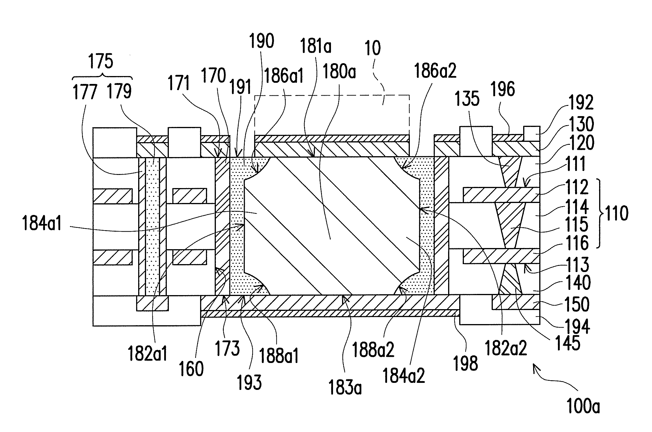
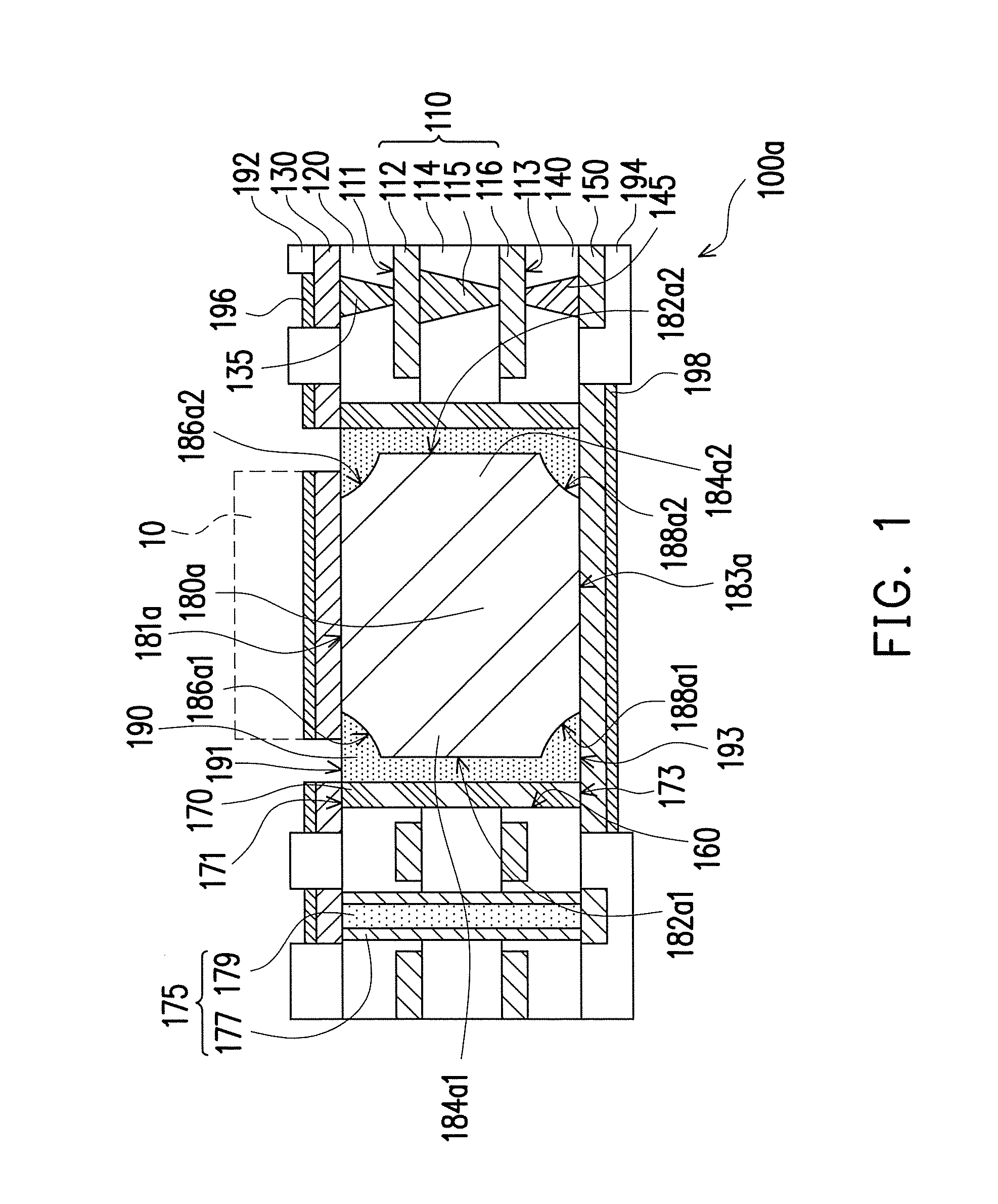
[0030]FIG. 1 is a cross-sectional view of a package carrier according to one embodiment of the present invention. Referring to FIG. 1, in the present embodiment, the package carrier 100a includes a substrate 110, a first insulation layer 120, a first patterned circuit layer 130, at least one first conductive through hole 135, a second insulation layer 140, at least one second conductive through hole 145, a second patterned circuit layer 150, a heat dissipation channel 160, a heat conducting element 180a and an adhesive layer 190.

[0031]Specifically, the substrate 110 has an upper surface 111 and a lower surface 113 opposite to each other. The first insulation layer 120 is disposed on the upper surface 111 of the substrate 110. The first patterned circuit layer 130 is disposed on the first insulation layer 120 and exposes a portion of the first insulation layer 120. The second insulation layer 140 is disposed on the lower surface 113 of the substrate 110. The second patterned circuit ...


PUM


Abstract

A package carrier includes a substrate, first and second insulation layers, first and second patterned circuit layers, at least one first and second conductive through holes, a heat dissipation channel, an adhesive layer and a heat conducting element. The first and second patterned circuit layers are respectively disposed on the first and second insulation layers which are respectively disposed on upper and lower surfaces of the substrate. The heat dissipation channel at least passes through the first insulation layer, the first and second patterned circuit layers, and the substrate. The first and second conductive through holes electrically connect with the substrate, the first and second patterned circuit layers. At least two opposite side surfaces of the heat conducting element each includes at least one convex portion or at least one concave portion. The heat conducting element is mounted in the heat dissipation channel via the adhesive layer.

Description

CROSS-REFERENCE TO RELATED APPLICATION[0001]This application claims the priority benefit of Taiwan application serial no. 101143964, filed on Nov. 23, 2012. The entirety of the above-mentioned patent application is hereby incorporated by reference herein and made a part of this specification.BACKGROUND OF THE INVENTION[0002]1. Field of the Invention[0003]The present invention relates to a substrate structure, and more particularly, to a package carrier.[0004]2. Description of Related Art[0005]In recent years, following the rapid development of electronic technology and emerging of high-tech electronic industries, high speed, multi-function, high density, light, small and low cost electronic products have been continuously introduced. These electronic products are usually provided with a package carrier. In addition to including a conductive circuit, such a package carrier may also carrier electronic elements as data processing units for the electronic products, such as, capacitors, ...

Claims


Application Information

Patent Timeline
Patent Type & Authority Applications(United States)
IPC IPC(8): H05K1/02
CPCH05K1/0206H01L2924/0002H05K2201/10416H05K2201/09154H01L2924/00
Inventor WANG, CHIN-SHENGCHEN, CHIEN-MING
Owner SUBTRON TECH
Why Eureka
Try Eureka