

Electro-optical device and electronic apparatus
a technology of optical devices and electronic devices, applied in non-linear optics, instruments, lenses, etc., can solve the problems of reducing yield, and affecting the illuminance of images projected on screens. achieve the effect of uniform illuminance of images
- Summary
- Abstract
- Description
- Claims
- Application Information
AI Technical Summary
Benefits of technology
Problems solved by technology
Method used
Image

Examples
first embodiment
Electro-Optical Device
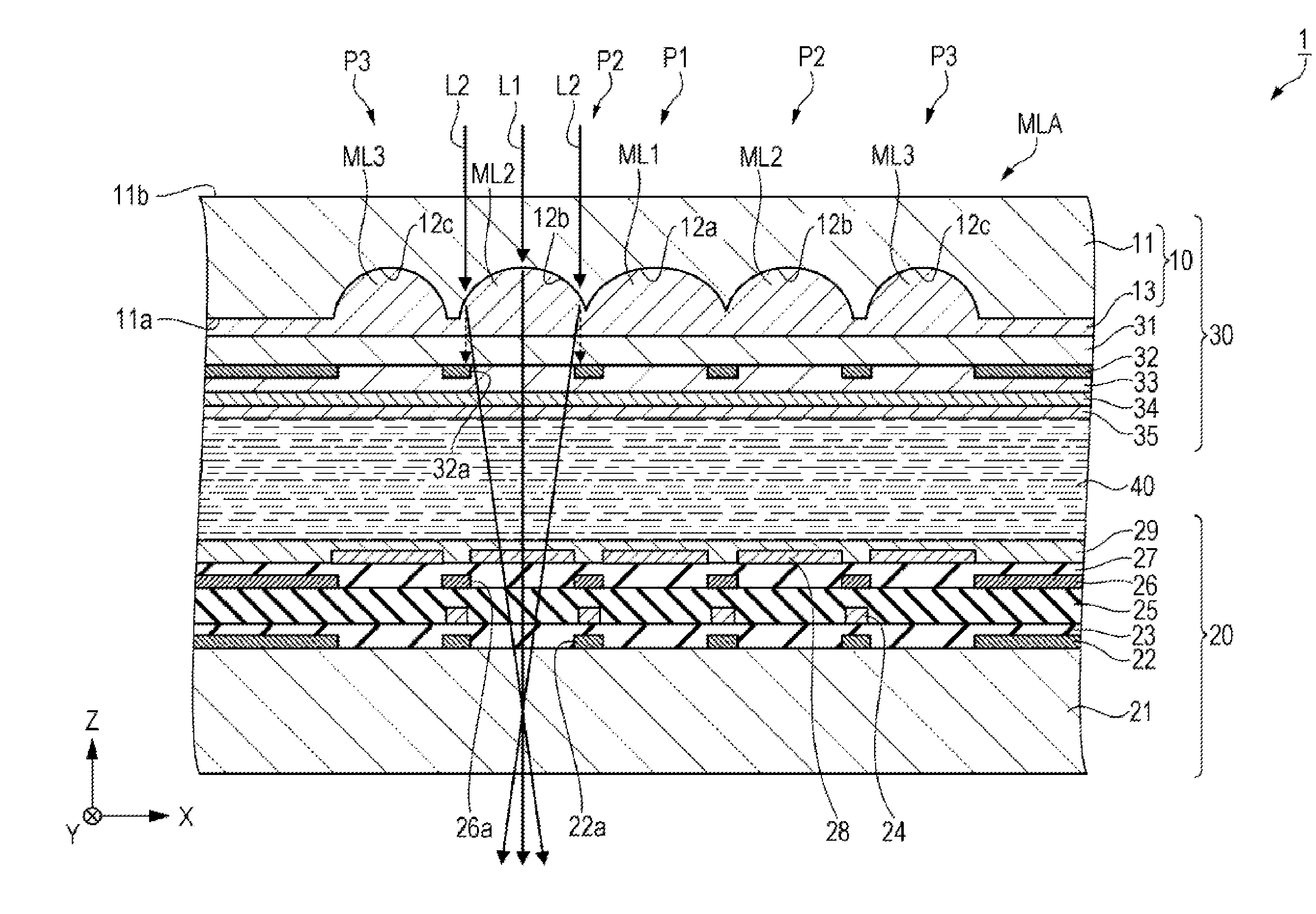
[0045]Here, as the electro-optical device, an active matrix-type liquid crystal device including a thin film transistor (TFT) as a switching element of a pixel will be described as an example. The liquid crystal device is able to be suitably used as a light modulating element (liquid crystal light valve) of a projection-type display device (projector) described later.
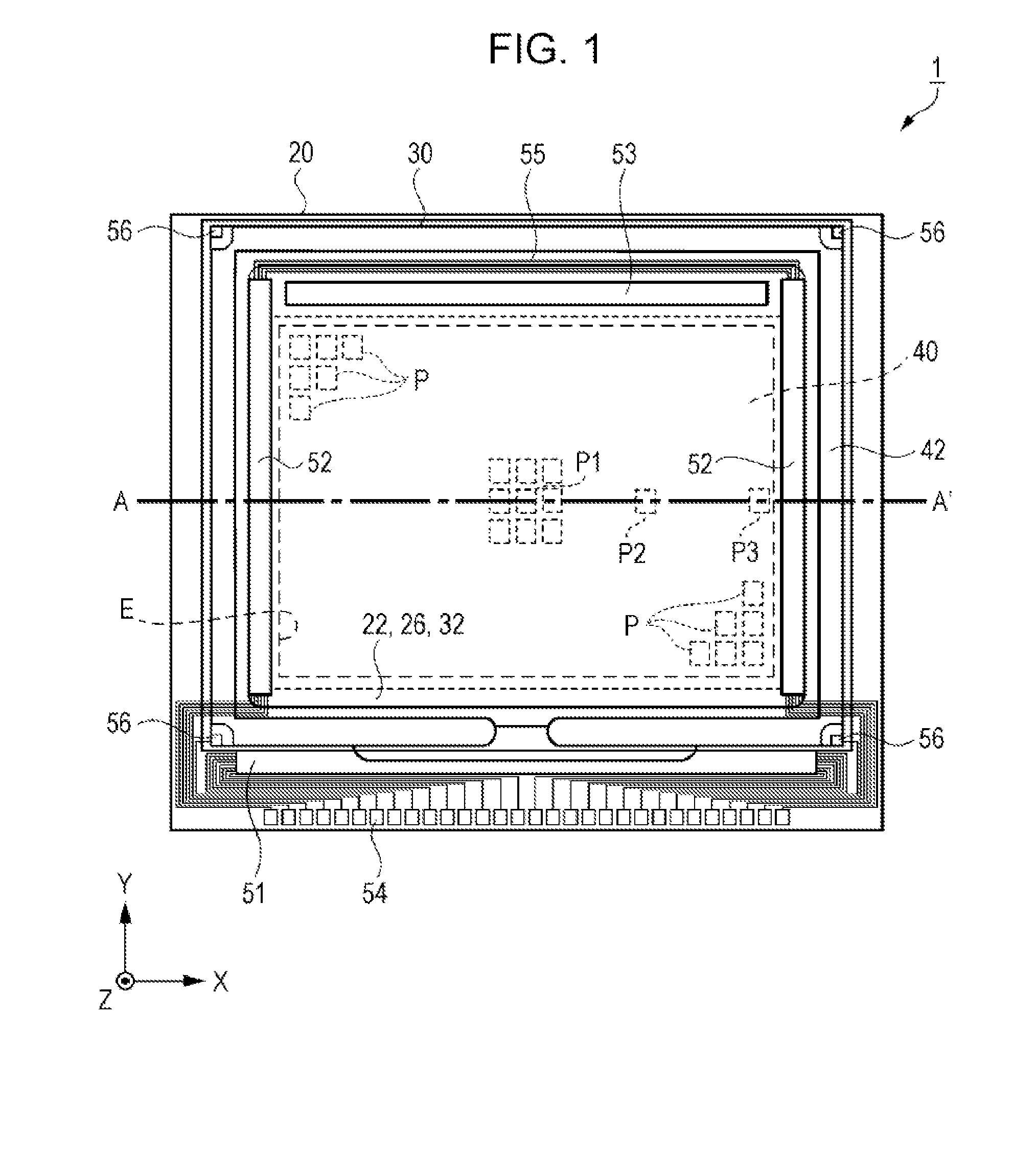
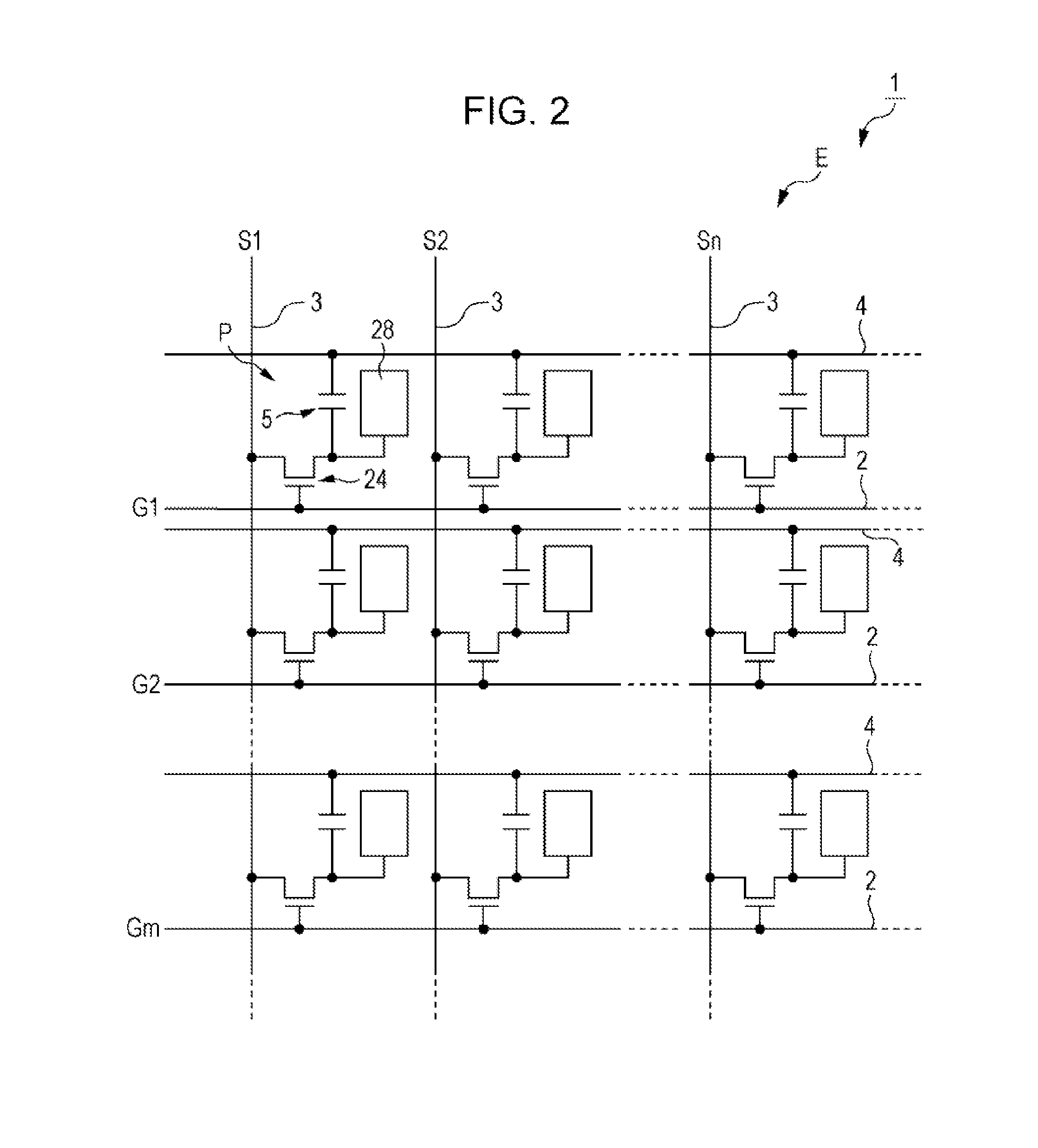
[0046]Firstly, a liquid crystal device as an electro-optical device according to the first embodiment will be described with reference to FIGS. 1, 2 and 3. FIG. 1 is a schematic plan view showing a configuration of a liquid crystal device according to a first embodiment. FIG. 2 is an equivalent circuit diagram showing an electrical configuration of a liquid crystal device according to the first embodiment. FIG. 3 is a schematic plan view showing a configuration of a liquid crystal device according to the first embodiment. More specifically, FIG. 3 is a schematic cross-sectional view taken along lin...
second embodiment
Liquid Crystal Device
[0122]The liquid crystal device according to the second embodiment differs with respect to the liquid crystal device according to the first embodiment on the point of including a microlens array substrate on both of the element substrate and the counter substrate; however, the other configurations are substantially the same. Here, constituent elements in common with the first embodiment are given the same reference numerals and will not be described.
[0123]A configuration of a liquid crystal device according to a second embodiment will be described. FIG. 8 is a schematic plan view showing a configuration of a liquid crystal device according to the second embodiment. More specifically, FIG. 8 is a schematic cross-sectional view taken along line A-A′ (X direction) in FIG. 1.
[0124]As shown in FIG. 8, the liquid crystal device 1A according to the second embodiment includes and microlens array substrate 10 on the counter substrate 30 similarly to the liquid crystal de...
third embodiment
Liquid Crystal Device
[0133]The liquid crystal device according to the third embodiment differs with respect to the liquid crystal device according to the first embodiment on the point of including two microlens array substrates the counter substrate; however, the other configurations are substantially the same. Here, constituent elements in common with the first embodiment are given the same reference numerals and will not be described.
[0134]In the liquid crystal device according to the third embodiment, with respect to the liquid crystal device according to the first embodiment, two microlens array substrates are included on the counter substrate, and the configuration of counter substrates is different. Here, the configuration of the counter substrates according to the third embodiment will be principally described. FIG. 9 is a schematic plan view showing a configuration of a liquid crystal device according to the third embodiment. FIG. 9 corresponds to a schematic cross-sectional...
PUM
 Abstract
Description
Claims
Application Information