Organic light emitting diode display having high luminescence

a light-emitting diode and organic technology, applied in the direction of thermoelectric device junction materials, electrical devices, semiconductor devices, etc., can solve the problems of difficult and/or rugged selection of organic light-emitting materials having enough permittivity, storage capacitance cannot be freely reduced as wanted, and the light-emitting area of organic light-emitting diodes can be enlarged, and the anode capacitance can be enhanced

Active Publication Date: 2014-06-12
LG DISPLAY CO LTD
View PDF23 Cites 2 Cited by
  • Summary
  • Abstract
  • Description
  • Claims
  • Application Information

AI Technical Summary

Benefits of technology

[0043]The organic light emitting diode display according to the present disclosure includes an additional capacitance connected to the anode capacitance of the organic light emitting diode in parallel. Especially, the additional capacitance has the structure in which the light emitting area of the organic light emitting diode display can be enlarged. Therefore, the present disclosure suggests an organic light emitting diode display having an enlarged light emitting area, ensuring enhanced the anode capacitance and representing brighter luminescence with the same power consumption. Further, the organic light emitting diode display according to the present disclosure includes the additional capacitance for enhancing the anode capacitance without enlarging the storage capacitance which may cause the lowered aperture ratio so that it can represent high luminescence without enlarging the pixel area and / or aperture ratio.

Problems solved by technology

The upper surface of the substrate having the color filter CF is not even and / or smooth, but may be uneven and / or rugged having many steps.
However, as the permittivity is the natural value of the material, it is very hard and restrictive to select organic light emitting material having enough permittivity we want.
Therefore, the storage capacitance cannot be reduced freely as wanted.
However, this method has another problem in that power consumption is increased.
It is very hard to design and manufacture an organic light emitting diode display with satisfying the various conditions at the same time, such as having lowered parasitic capacitance, ensuring enough storage capacitance, and having higher aperture ratio.

Method used


Image

  • Organic light emitting diode display having high luminescence
  • Organic light emitting diode display having high luminescence
  • Organic light emitting diode display having high luminescence

Examples


first embodiment

[0062]In order not to affect to the aperture ratio with satisfying the equivalent circuit diagram shown in FIG. 5, the additional capacitance Cnew according to the present disclosure may be formed by overlapping the anode electrode ANO with the driving current line VDD connected to the source electrode DS of the driving thin film transistor DT. Hereinafter, referring to FIGS. 6 and 7, we will explain about an organic light emitting diode display according to the present disclosure. FIG. 6 is a plane view illustrating a bottom emission type organic light emitting diode display according to the present disclosure. FIG. 7 is a cross sectional view along the cutting line of II-II′ in FIG. 6 for illustrating the structure of a bottom emission type organic light emitting diode display according to the present disclosure.

[0063]The bottom emission type active matrix organic light emitting diode display according to the first embodiment of the present disclosure includes a switching thin fil...

second embodiment

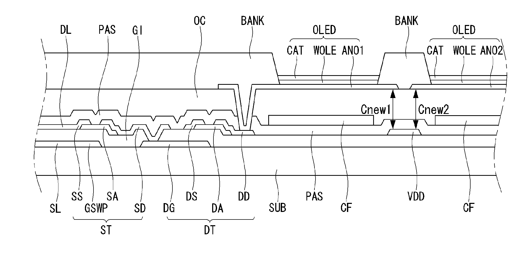
[0086]In the interim, for the case of the second embodiment, one driving current line VDD is allocated at the neighbored two pixel columns. Therefore, the first anode electrode ANO1 disposed at one side (left side) pixel area overlaps with one side portion (right side portion) of the driving current line VDD to form the first additional capacitance Cnew1. Like that, the second anode electrode ANO2 disposed at other side (right side) pixel area overlaps with other side portion (left side portion) of the driving current line VDD to form the second additional capacitance Cnew2.


PUM


Abstract

The present disclosure relates to an organic light emitting diode display having high luminescence. The present disclosure suggests an organic light emitting diode display comprising: a data line, a scan line and a driving current line defining a pixel area on a substrate; an anode electrode formed within the pixel area; an additional capacitance formed by overlapping expanded portions of the anode electrode with some portions of the driving current line; a bank defining a light emitting area in the anode electrode; an organic emission layer formed on the anode electrode; and a cathode electrode formed on the organic emission layer. The present disclosure suggests high luminescence organic light emitting diode display by including an additional capacitance for increasing the anode capacitance.

Description

CROSS-REFERENCE TO RELATED APPLICATIONS[0001]This application claims the benefit of Korea Patent Application No. 10-2012-0144813 filed on Dec. 12, 2012, which is incorporated herein by reference for all purposes as if fully set forth herein.BACKGROUND[0002]1. Field of the Invention[0003]The present disclosure relates to an organic light emitting diode display having high luminescence. Especially, the present disclosure relates to an organic light emitting diode display having high luminescence with low power consumption by enhancing the capacity of anode electrode and the capacitance of organic light emitting diode itself.[0004]2. Discussion of the Related Art[0005]Nowadays, various flat panel display devices are developed for overcoming many drawbacks of the cathode ray tube such as heavy weight and bulk volume. The flat panel display devices include the liquid crystal display device (or LCD), the field emission display (or FED), the plasma display panel (or PDP) and the electrolum...

Claims


Application Information

Patent Timeline
Patent Type & Authority Applications(United States)
IPC IPC(8): H01L27/32
CPCH10K59/1216H10K59/121H10K59/123H10K59/131H10K50/30H01L27/1255
Inventor JUNG, KIMOONHWANG, SOONJAESHIM, JONGSIK
Owner LG DISPLAY CO LTD
Why Eureka
Try Eureka