Current breaker and wireless communication device having the same

a technology of wireless communication device and current breaker, which is applied in the field of antenna, can solve the problems of large area, lack of practicality, and interference with the original characteristics of the antenna, and achieve the effect of the current breaker

Active Publication Date: 2014-06-12
REALTEK SEMICON CORP
View PDF4 Cites 6 Cited by
  • Summary
  • Abstract
  • Description
  • Claims
  • Application Information

AI Technical Summary

Benefits of technology

[0007]The object of the present invention is to provide a current breaker and a wireless communication device having the same. A parallel resonant LC circuit comprises inductors and capacitors of printed type and acts as an open circuit at a resonant frequency, thus the circuit could block the flowing of current along the edge of the ground plane on the substrate to achieve the efficacy of the current breaker.
[0011]In summary, by means of an open circuit effect achieved by current breakers operated at a resonant frequency, the current breakers and the wireless communication device having the current breakers in the embodiment of the present invention could block current's flowing on the ground plane, so as to reduce the affect which the current on the ground plane has on the antenna.

Problems solved by technology

In general microwave circuits, electrical current flows along the edge of the ground plane of a substrate, resulting in additional radiation that interferes with the original characteristics of an antenna.
Related designs of a current breaker were therefore incorporated in today's communication products, however, with a lack of practicality due to the need of a large area.
However, in this manner it is unpractical and less useful since the component size of the current breaker 12 is roughly equal to quarter wavelength corresponding to the operation frequency, resulting in the need of a large area.
However, the occupied area of proposed architecture is too large.
In practical application, a complete area of the ground plane will not be added to this design, so this design does not make a substantial contribution to the reduction of size of the components.

Method used


Image

  • Current breaker and wireless communication device having the same
  • Current breaker and wireless communication device having the same
  • Current breaker and wireless communication device having the same

Examples


Embodiment Construction

[0028]The aforementioned illustrations and following detailed descriptions are exemplary for the purpose of further explaining the scope of the present invention. Other objectives and advantages related to the present invention will be illustrated in the subsequent descriptions and appended drawings.

[0029][Embodiment of a Current Breaker and a Wireless Communication Device Having the Same]

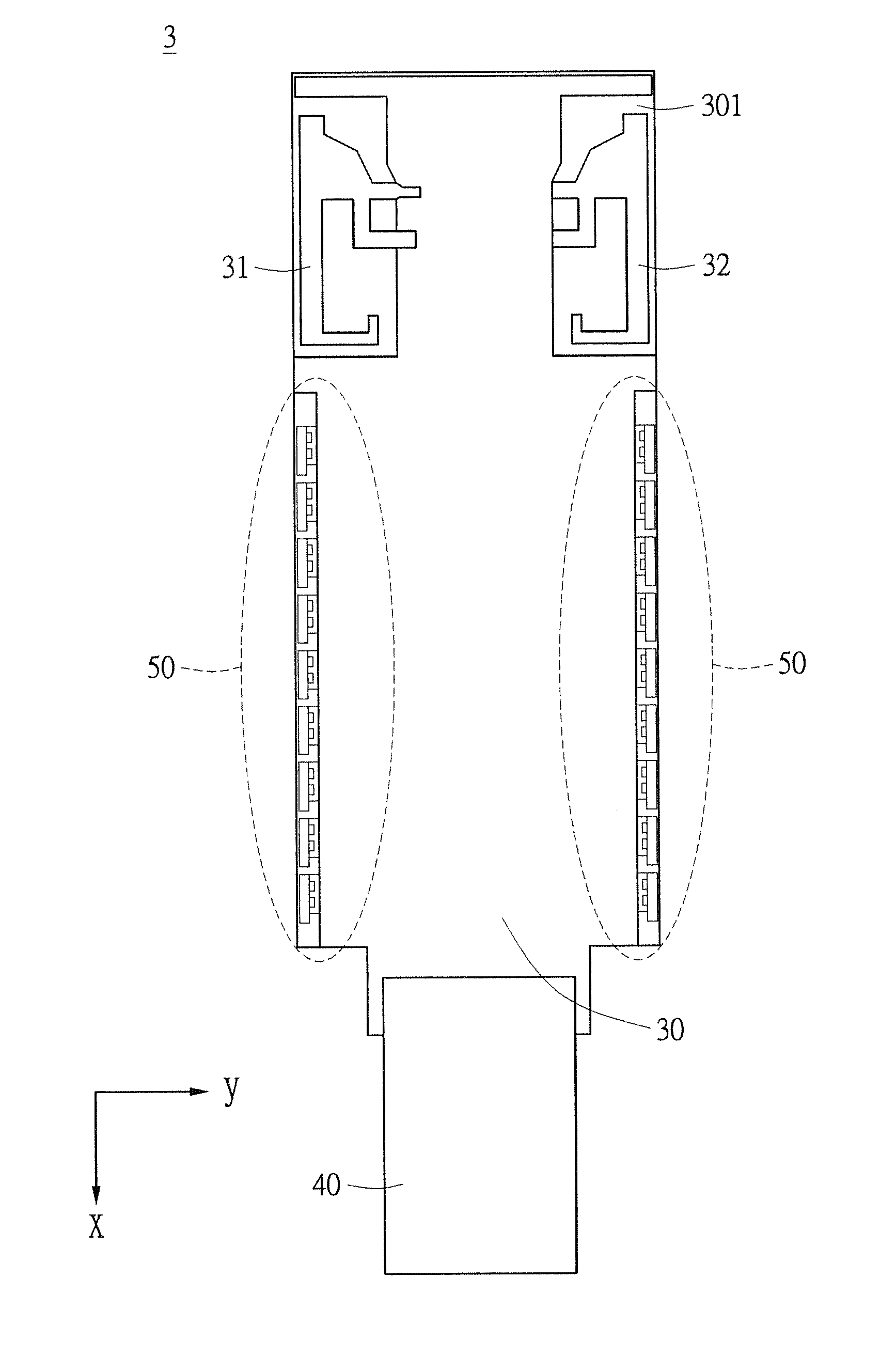
[0030]The present invention proposes an innovative design of a wireless communication device having current breakers. The design incorporates an antenna and current breakers, wherein the antenna adopts the design of planar inverted-F antenna (PIFA); and a plurality of current breaker structures are jointed on two side edges of the ground plane thereof. The image current generated at the edges of the ground plane by the antenna body will provide the antenna with additional radiation, thereby interfering with the original characteristic of the antenna.

[0031]FIG. 3A is a schematic view showing a wirel...


PUM


Abstract

A current breaker comprises a multi-layer printed circuit board (PCB), a ground plane, a metal component and a conductive via hole. The ground plane is disposed in a first metal layer of the multi-layer PCB and comprises a slot forming inductive impedance. The slot comprises an extended portion. The metal component is disposed in a second metal layer of the multi-layer PCB. Capacitive impedance is formed between the metal component and the ground plane. The projection of the metal component on the ground plane and the extended portion of the slot partially overlap. The conductive via hole penetrates the multi-layer PCB to connect metal component with the ground plane. The first and the second metal layers are any two metal layers of the multi-layer PCB. The inductive impedance formed by the slot and the capacitive impedance formed between the metal component and the ground plane create a parallel LC equivalent circuit.

Description

BACKGROUND OF THE INVENTION[0001]1. Field of the Invention[0002]The present invention relates to an antenna; in particular, to current breakers of antenna structures and wireless communication devices having the same.[0003]2. Description of Related Art[0004]In general microwave circuits, electrical current flows along the edge of the ground plane of a substrate, resulting in additional radiation that interferes with the original characteristics of an antenna. Related designs of a current breaker were therefore incorporated in today's communication products, however, with a lack of practicality due to the need of a large area.[0005]Reference is made to FIG. 1. FIG. 1 is a schematic view showing a traditional one quarter wavelength current breaker, and the proposed method is related to a traditional current breaker with one quarter wavelength. Please refer to the reference: Peter Lindberg and Erik Öjefors, “A Bandwidth Enhancement Technique for Mobile Handset Antennas Using Wavetraps,...

Claims


Application Information

Patent Timeline
Patent Type & Authority Applications(United States)
IPC IPC(8): H01Q1/48H03H7/01
CPCH01Q1/48H01P1/20345H01Q1/243H01Q1/521H05K1/0225H05K1/0233H05K1/0236H05K1/0251H05K1/16H05K2201/09672H05K2201/09781
Inventor WANG, SY-BEENLIN, CHIH-PAOLING, CHING-WEI
Owner REALTEK SEMICON CORP
Why Eureka
Try Eureka