Thin film transistor array panel and method of manufacturing the same

a technology array panels, which is applied in the direction of semiconductor/solid-state device manufacturing, electrical equipment, semiconductor devices, etc., can solve the problems of difficult control of etching profiles, poor product quality, and deterioration of the characteristics of thin film transistors that use such wiring

Active Publication Date: 2014-06-26
SAMSUNG DISPLAY CO LTD
View PDF3 Cites 20 Cited by
  • Summary
  • Abstract
  • Description
  • Claims
  • Application Information

AI Technical Summary

Benefits of technology

[0032]According to the exemplary embodiments, it is possible to prevent damage from occurring during a subsequent process by removing a projection of metal oxide formed after wet etching when a capping layer including metal oxide is used.

Problems solved by technology

There is a problem, however, in that the characteristics of the thin film transistor that uses such wiring can deteriorate due to a reaction between the main wiring layer formed of metal and other layers in a process, and the like.
But it is difficult to control an etching profile when a capping layer is used due to a difference between the etching speeds of the main wiring layer and the capping layer, and thus the resulting quality of the product may be poor due to problems that may occur during subsequent processing.

Method used


Image

  • Thin film transistor array panel and method of manufacturing the same
  • Thin film transistor array panel and method of manufacturing the same
  • Thin film transistor array panel and method of manufacturing the same

Examples


Embodiment Construction

[0036]Hereinafter, exemplary embodiments will be described in detail with reference to the accompanying drawings. As those with ordinary skill in the art would realize, the described embodiments may be modified in various different ways, all without departing from the spirit or scope of the present disclosure. On the contrary, exemplary embodiments introduced herein are provided to sufficiently transfer the spirit of the present disclosure to persons of ordinary skill in the art.

[0037]In the drawings, the thickness of layers, films, panels, regions, etc., are exaggerated for clarity. It will be understood that when a layer is referred to as being “on” another layer or substrate, it can be directly on the other layer or substrate, or an intervening layer or substrate may also be present. Like reference numerals designate like elements throughout the specification.

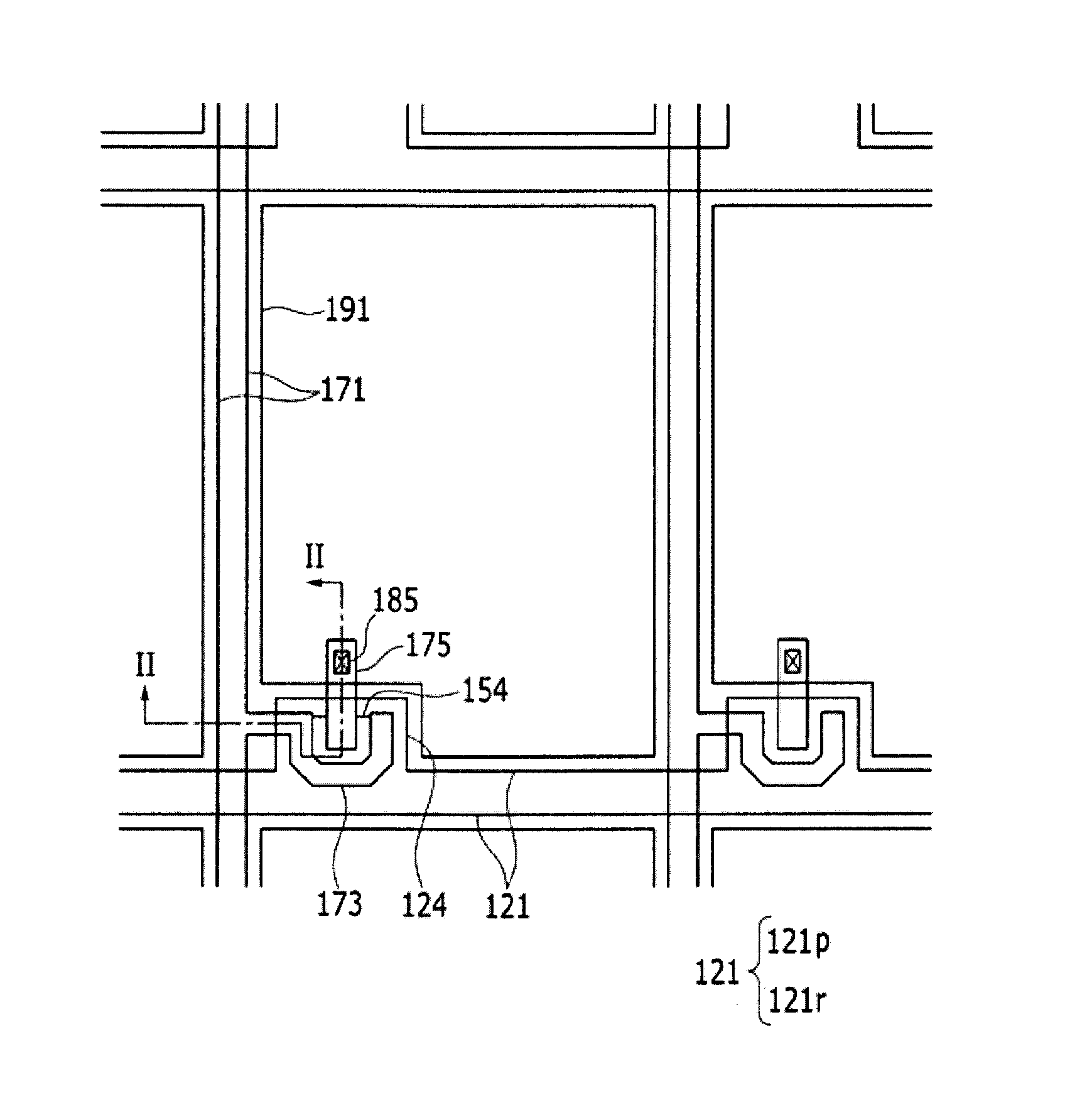
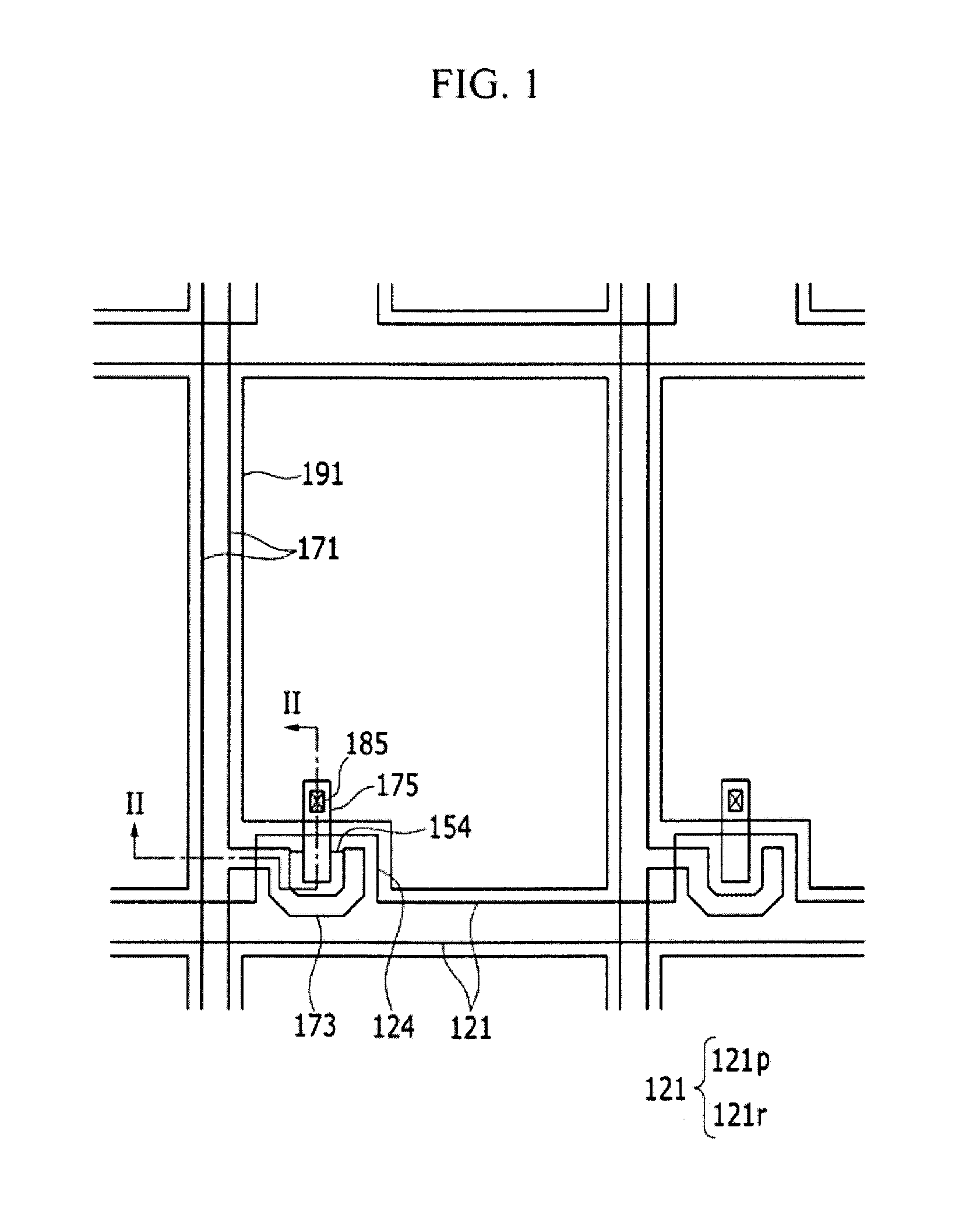
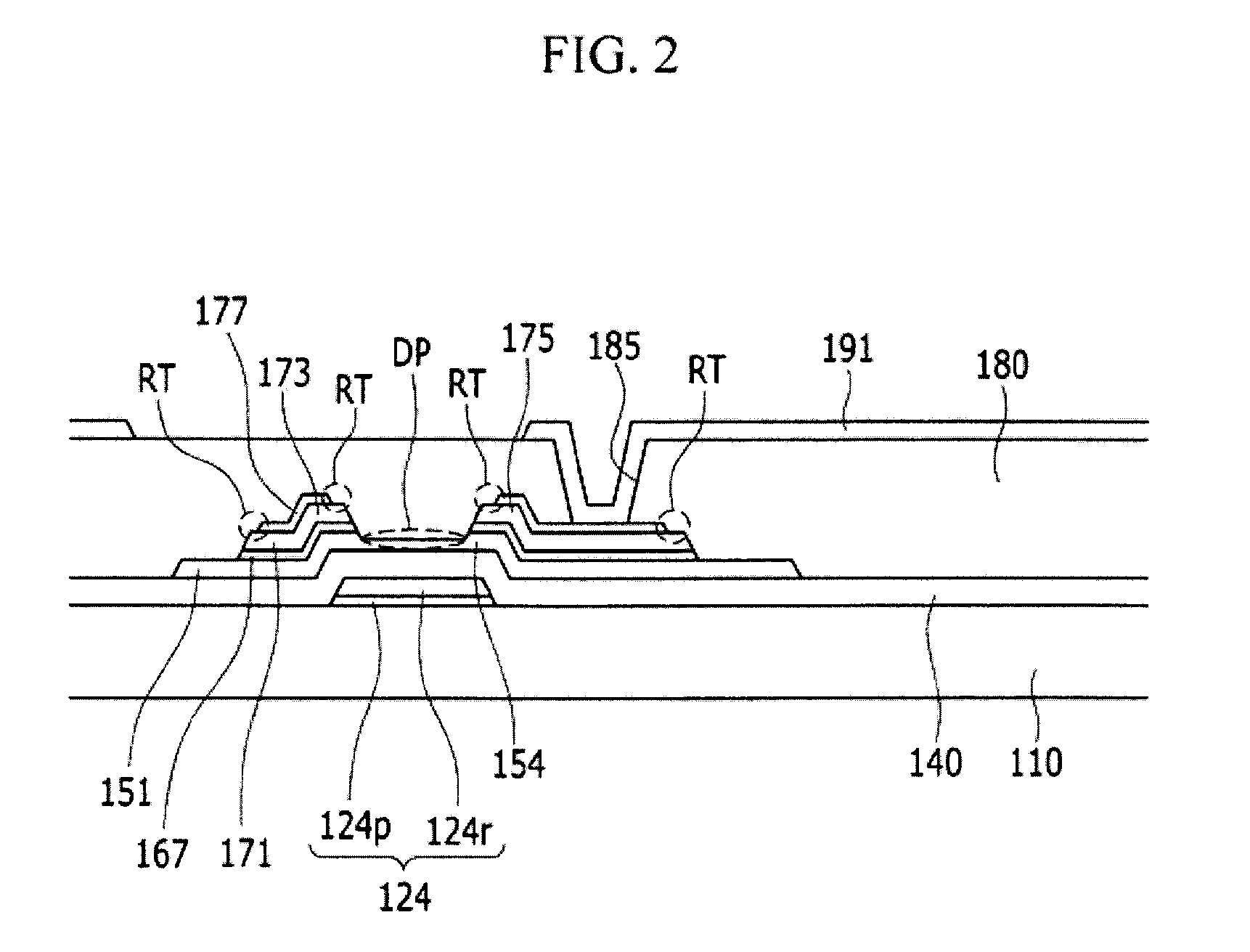
[0038]FIG. 1 is a top plan view illustrating a thin film transistor array panel according to an exemplary embodiment. FIG....


PUM


Abstract

A thin film transistor array panel includes: a substrate, a gate line positioned on the substrate and including a gate electrode, a semiconductor layer positioned on the substrate and including an oxide semiconductor, a data wire layer positioned on the substrate and including a data line crossing the gate line, a source electrode connected to the data line, and a drain electrode facing the source electrode, and a capping layer covering the data wire layer, in which an end of the capping layer is inwardly recessed as compared to an end of the data wire layer.

Description

CROSS-REFERENCE TO RELATED APPLICATION[0001]This application claims priority to and the benefit of Korean Patent Application No. 10-2012-0152153 filed in the Korean Intellectual Property Office on Dec. 24, 2012, the entire contents of which are incorporated herein by reference.BACKGROUND[0002](a) Technical Field[0003]The present invention relates to a thin film transistor array panel and a method of manufacturing the same.[0004](b) Description of the Related Art[0005]In general, flat panel displays such as liquid crystal displays or organic light emitting displays include a plurality of pairs of field generating electrodes and an electro-optical active layer interposed therebetween. In the case of liquid crystal displays, a liquid crystal layer is included as the electro-optical active layer, and in the case of organic light emitting displays, an organic emission layer is included as the electro-optical active layer.[0006]One of the field generating electrodes of the pair is general...

Claims


Application Information

Patent Timeline
Patent Type & Authority Applications(United States)
IPC IPC(8): H01L33/00
CPCH01L21/77H01L29/41733H01L29/45H01L29/66969H01L29/7869H01L27/1225H01L27/124H01L27/1288
Inventor CHOI, SHIN ILKIM, SANG GABKONG, HYANG-SHIKBAE, SU BINJEONG, YU-GWANG
Owner SAMSUNG DISPLAY CO LTD
Why Eureka
Try Eureka