
Magnetoresistive memory device and fabrictaion method

Inactive Publication Date: 2014-06-26
SEMICON MFG INT (SHANGHAI) CORP
View PDF10 Cites 5 Cited by
  • Summary
  • Abstract
  • Description
  • Claims
  • Application Information

AI Technical Summary

Benefits of technology

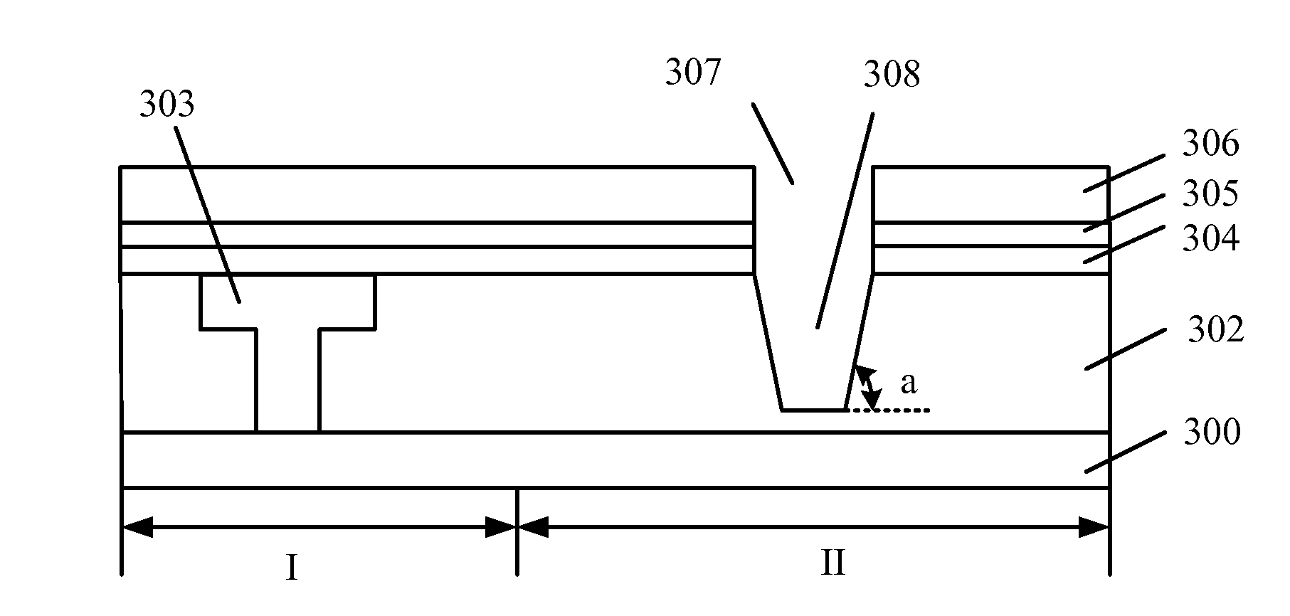
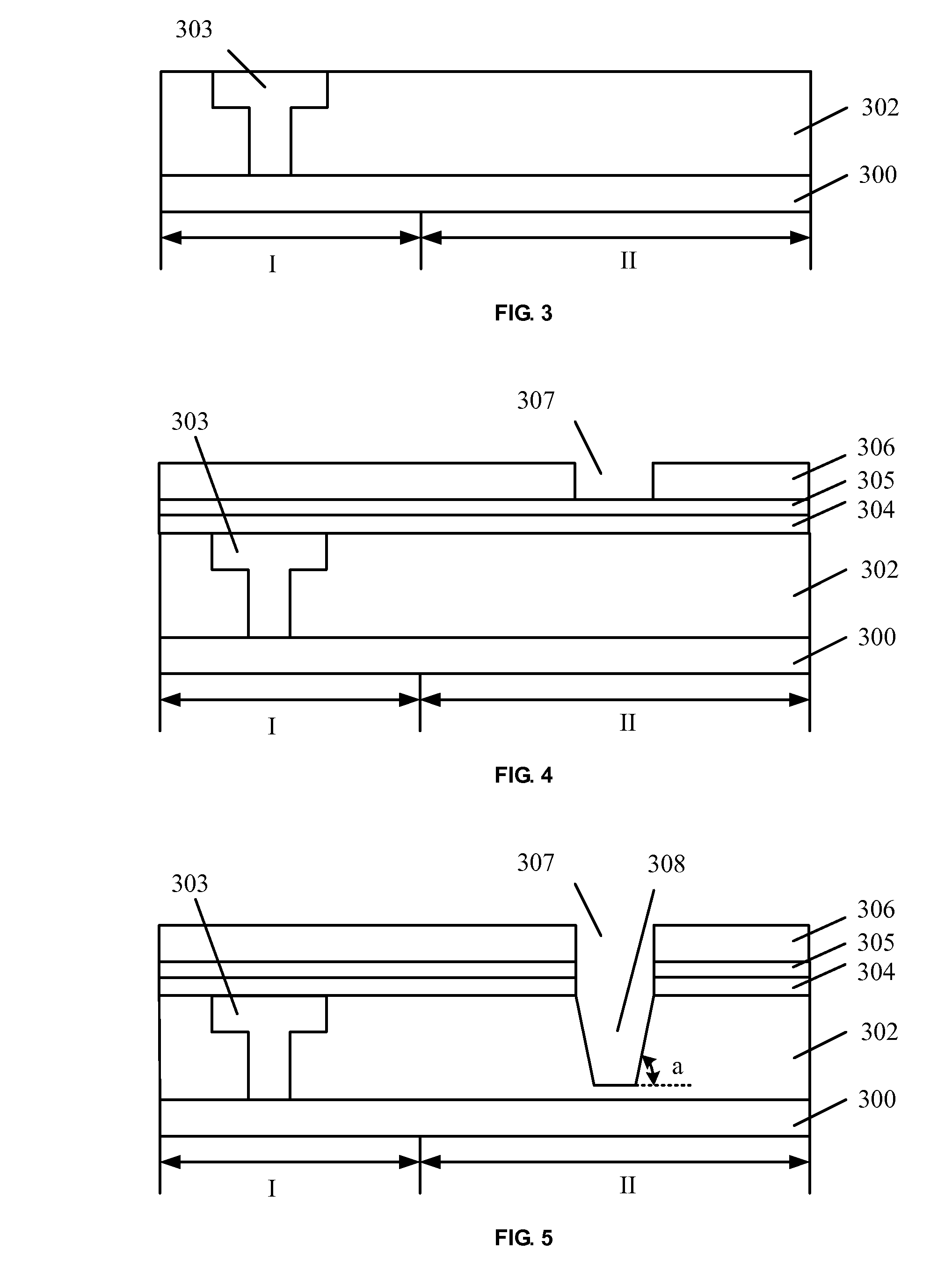
The present patent discloses a magnetoresistive memory device and its fabrication method that can be made using a CMOS compatible process. The device includes a first dielectric layer with a groove, a first metal layer that fills the groove and serves as a programming line for a magnetic tunnel junction, a cobalt metal layer between the first metal layer and the groove, and a magnetic tunnel junction. The device also includes a second dielectric layer between the magnetic tunnel junction and the cobalt metal layer. The fabrication method includes etching the groove with a controlled angle to minimize protrusions and form a better surface. The technical effect of this patent is to provide a reliable and efficient method for fabricating a magnetoresistive memory device that can be used in various electronic devices.

Problems solved by technology

However, when programming existing magnetoresistive memory devices, the first programming line often requires a high drive current.
This adversely affects stability of the devices and increasing degree of device integration.

Method used


Image

  • Magnetoresistive memory device and fabrictaion method
  • Magnetoresistive memory device and fabrictaion method
  • Magnetoresistive memory device and fabrictaion method

Examples


Embodiment Construction

[0016]Reference will now be made in detail to exemplary embodiments of the disclosure, which are illustrated in the accompanying drawings. Wherever possible, the same reference numbers will be used throughout the drawings to refer to the same or like parts. For illustration purposes, the schematic drawings may be not to scale. The schematic drawings are solely illustrative, and should not limit the scope of the present disclosure. In addition, three-dimensional scales of length, width and depth should be included in practical fabrication process.

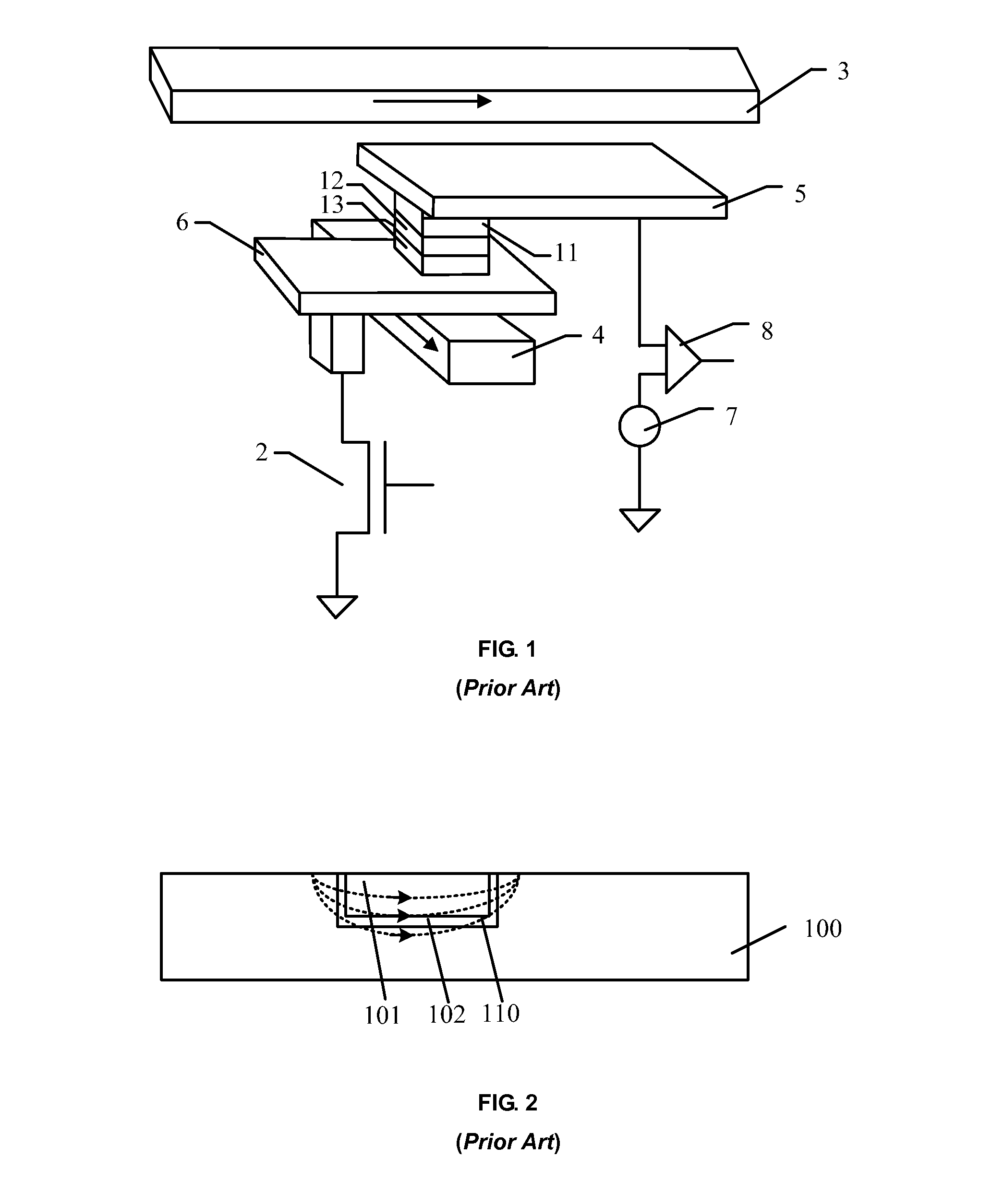
[0017]During programming of existing magnetoresistive memory devices, the first programming line often requires a high drive current. FIG. 2 depicts a cross-sectional view of a first programming line of a conventional magnetoresistive memory device. The first programming line includes: a substrate 100, a metal layer 101 located in the substrate 100, and a barrier layer 102 located between the metal layer 101 and the substrate 100. The metal ...


PUM


Abstract

A magnetoresistive memory device and a fabrication method are provided. A first dielectric layer disposed on a semiconductor substrate can include a groove formed therein. A cobalt metal layer can be formed over a bottom surface and a sidewall surface of the groove. A first metal layer can be formed over the cobalt metal layer. The first metal layer can fill the groove and be used as a first programming line of the magnetoresistive memory device. A second dielectric layer can be formed over the first dielectric layer and over the first metal layer. A magnetic tunnel junction can be formed over the second dielectric layer. The magnetic tunnel junction can be positioned corresponding to a position of the first metal layer. The magnetic tunnel junction can include an insulating layer sandwiched between a lower magnetic material layer and an upper magnetic material layer.

Description

CROSS-REFERENCES TO RELATED APPLICATIONS[0001]This application claims priority to Chinese Patent Application No. CN201210559867.1, filed on Dec. 20, 2012, the entire contents of which are incorporated herein by reference.FIELD OF THE DISCLOSURE[0002]The present disclosure relates to the field of semiconductor technology and, more particularly, relates to a magnetoresistive memory device and fabrication method.BACKGROUND[0003]Magnetoresistive memory (e.g., magnetoresistive random access memory, MRAM) is a non-volatile memory (NVM) characterized with high integration density, high responding speed and write endurance. The magnetoresistive memory may become a mainstream product among storage devices with the advancement of processes, compared with a flash memory. The feature size of a flash memory cannot be infinitely reduced.[0004]A main component of a magnetoresistive memory device is a magnetic tunnel junction (MTJ). The most simplified magnetic tunnel junction consists of a three-l...

Claims


Application Information

Patent Timeline
IPC IPC(8): H01L43/12H01L43/02
CPCH10N50/01H10N50/10
Inventor CHEN, WENFUHE, PAULZHANG, ALFREDSHI, SEN
Owner SEMICON MFG INT (SHANGHAI) CORP
Learn More