Focal plane array with pixels defined by modulation of surface fermi energy

a technology of fermi energy and modulation, applied in the field of optical plane arrays with modulation pixels, can solve the problems of surface leakage current and significant complexity of fabrication, and achieve the effect of simplifying the fabrication process and minimizing the possibility of detrimental surface leakag

Active Publication Date: 2014-07-10
SUNDARAM MANI +1
View PDF2 Cites 19 Cited by
  • Summary
  • Abstract
  • Description
  • Claims
  • Application Information

AI Technical Summary

Benefits of technology

[0005]Embodiments address these needs with a focal plane array (FPA) where the pixels are defined, not by the usual methods of selective diffusion or selective ion-implantation or etching trenches (i.e. removing detector material between pixels), but by a deliberate and controlled variation of the Fermi energy at the surface of the detector array. Embodiments dispense entirely with any deep etching to delineate individual pixels. They rely, inst

Problems solved by technology

There are significant drawbacks to the requirement that trenches be etched in a two-dimensional mesa pattern in order to define individual pixels.
First, the fabrication becomes signific

Method used


Image

  • Focal plane array with pixels defined by modulation of surface fermi energy
  • Focal plane array with pixels defined by modulation of surface fermi energy
  • Focal plane array with pixels defined by modulation of surface fermi energy

Examples


Embodiment Construction

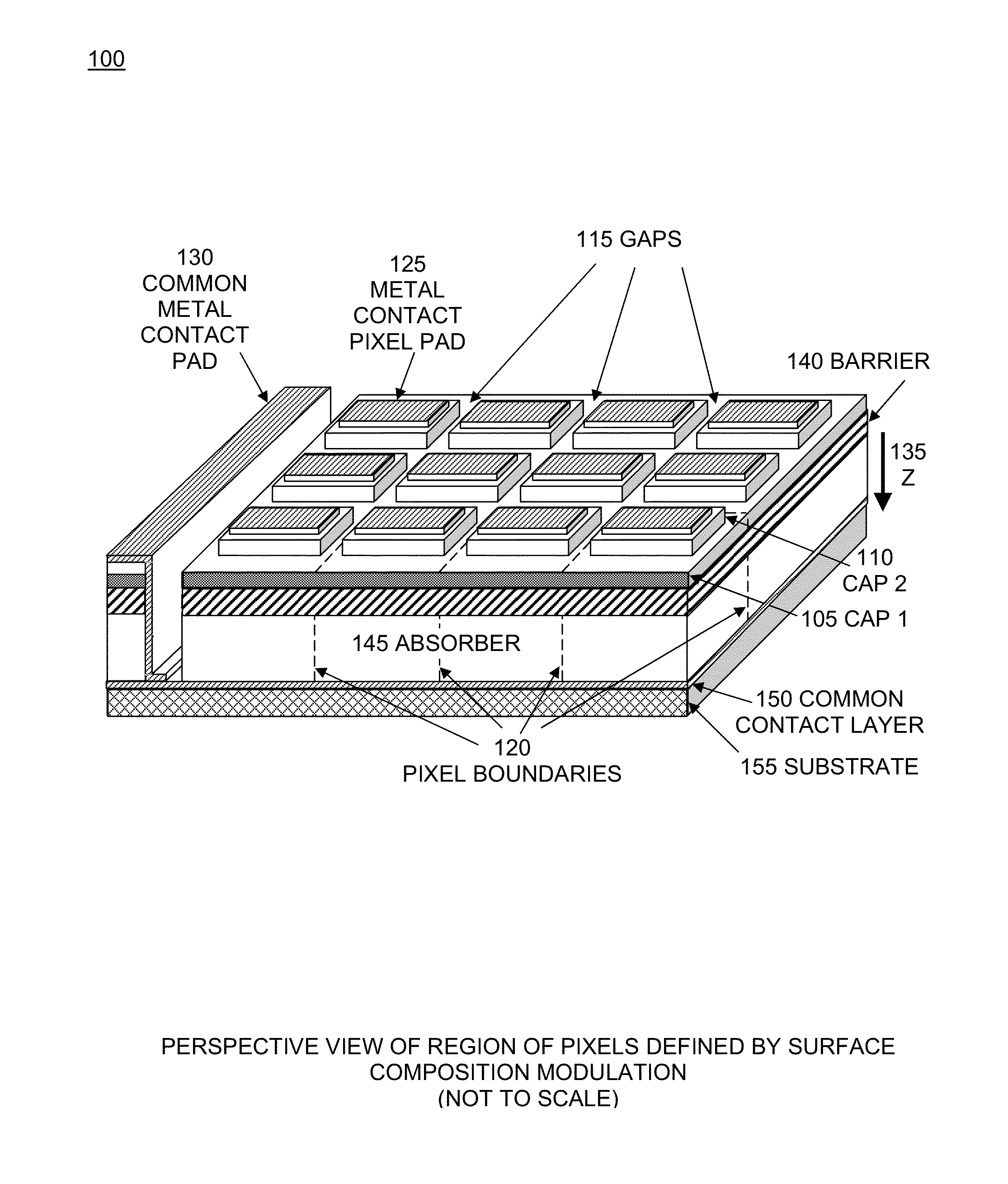
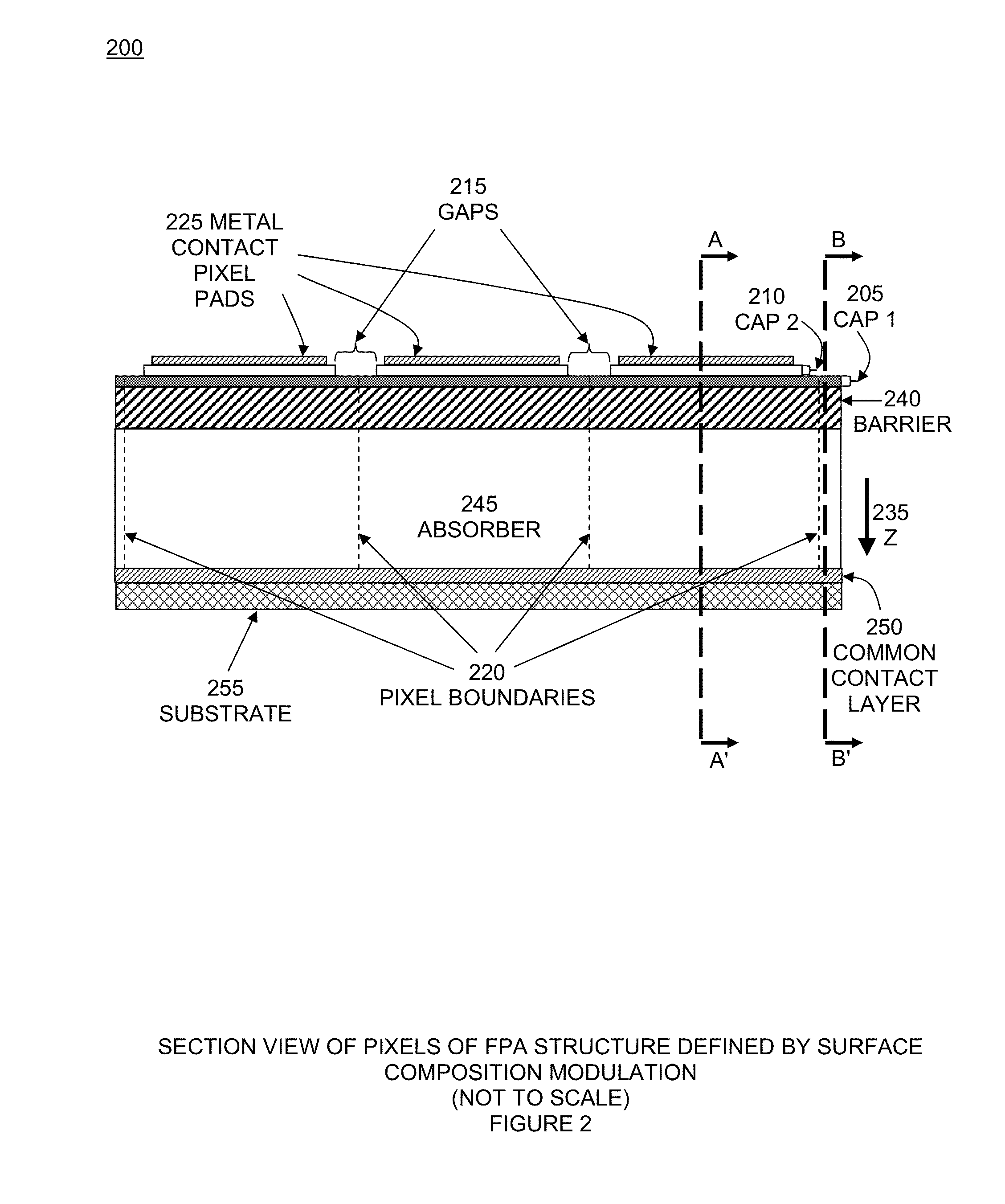
[0020]Embodiments comprise a method of surface Fermi energy modulation by a controlled variation of the chemical composition of the detector surface. The Fermi energy level at which the free surface of a semiconductor is pinned with respect to its energy bandgap is unique to that semiconductor and varies from one semiconductor to another; it is a function of surface states which, in turn, depend on the density and composition of surface oxides as well as surface dangling bonds. The net result is the presence at the surface and some distance below it of a net excess of charge carriers (electrons or holes) or a net depletion of them.

[0021]Varying the chemical composition of the semiconductor at a detector surface produces a corresponding variation in the surface Fermi energy (e.g. 250 meV in amplitude) which, in turn, produces a corresponding variation in the electric field and electrostatic potential in the bulk semiconductor below the surface. Embodiments exploit this effect to defi...


PUM


Abstract

Pixels in a focal plane array are defined by controlled variation of the Fermi energy at the surface of the detector array. Varying the chemical composition of the semiconductor at the detector surface produces a corresponding variation in the surface Fermi energy which produces a corresponding variation in the electric field and electrostatic potential in the bulk semiconductor below the surface. This defines pixels by having one Fermi energy at the surface of each pixel and a different Fermi energy at the surface between pixels. Fermi energy modulation can also be controlled by applying an electrostatic potential voltage V1 to the metal pad defining each pixel, and applying a different electrostatic potential voltage V2 to an interconnected metal grid covering the gaps between all the pixel metal pads. Methods obviate the need to etch deep trenches between pixels, resulting in a more manufacturable quasi-planar process without sacrificing performance.

Description

RELATED APPLICATIONS[0001]This application claims the benefit of U.S. Provisional Application No. 61 / 748,958, filed Jan. 4, 2013. This application is herein incorporated in its entirety by reference.FIELD OF THE INVENTION[0002]The invention relates to focal plane array (FPA) sensors, and more particularly, to a focal plane array with pixels defined by modulation of surface Fermi energy.BACKGROUND OF THE INVENTION[0003]Focal plane arrays typically consist of two dimensional arrays of individual and separate detectors—or pixels—which must be physically isolated from one another (mesas) in order to be able to generate an image of a scene devoid of any crosstalk or signal admixture between adjacent pixels. The detectors themselves are commonly made of an appropriate semiconductor material, regions of which can be doped either p-type or n-type. The junction between regions of opposite doping characters forms a so-called p-n photodiode which has the important ability to generate an electr...

Claims


Application Information

Patent Timeline
IPC IPC(8): H01L27/146H01L31/0352
CPCH01L27/1463H01L27/14683H01L31/035236H01L31/022408H01L31/109
Inventor SUNDARAM, MANIREISINGER, AXEL
Owner SUNDARAM MANI
Why Eureka
Try Eureka