

Self-aligned dielectric isolation for finfet devices
- Summary
- Abstract
- Description
- Claims
- Application Information
AI Technical Summary
Benefits of technology
Problems solved by technology
Method used
Image

Examples
Embodiment Construction
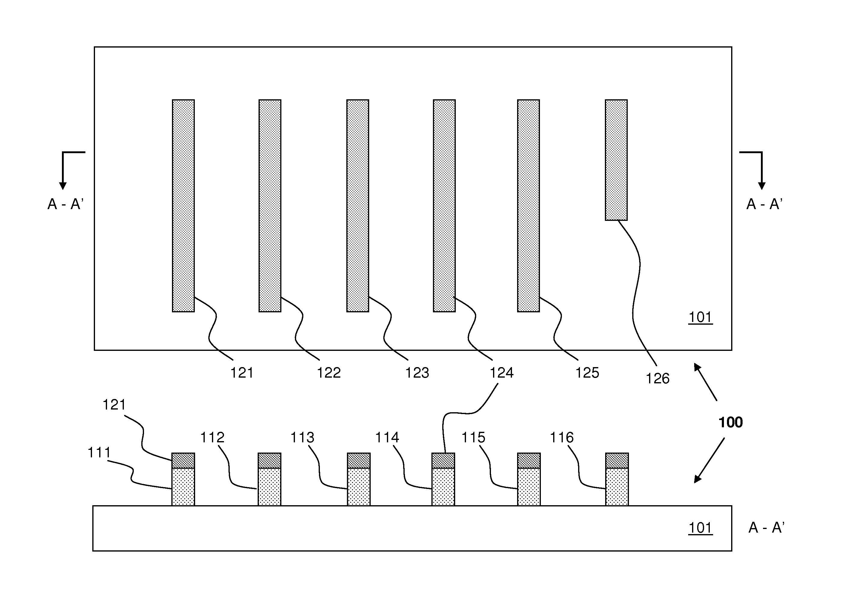
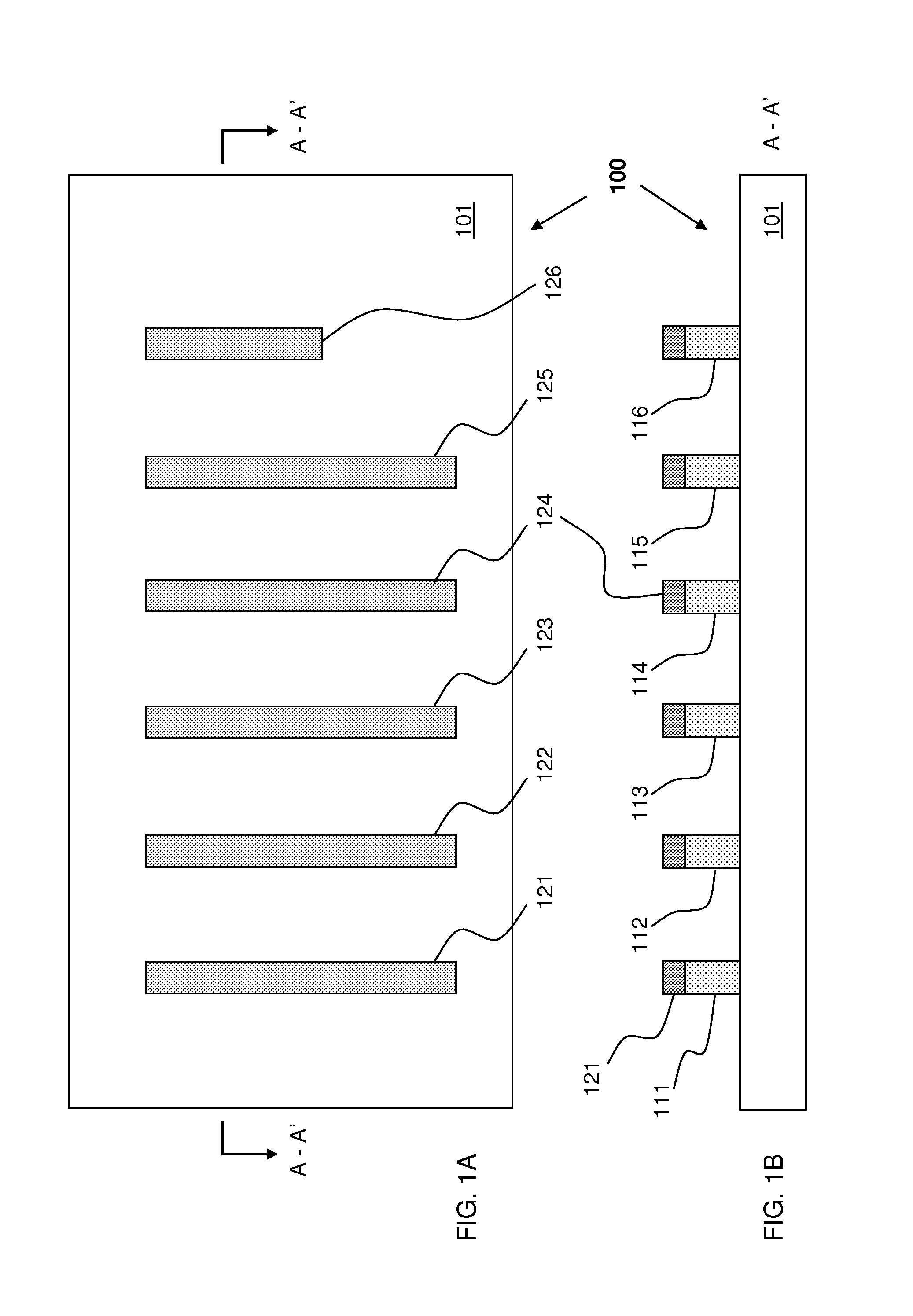
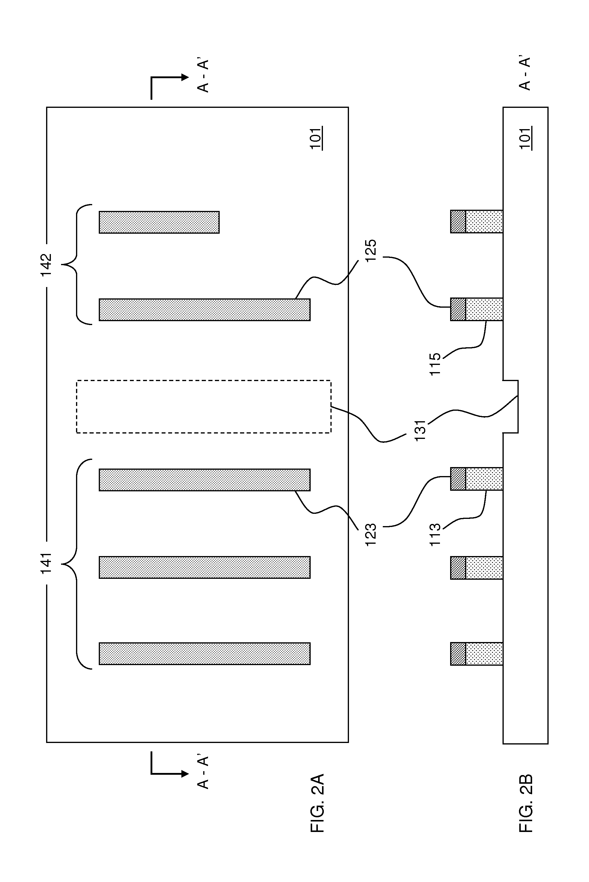
[0004]Embodiments of the present invention provide a method of form a semiconductor structure, and in particular an insulating structure surrounding a set of fins of one or more fin-type field-effect-transistors (FinFETs). The method includes forming a set of device features on top of a substrate; forming a first dielectric layer directly on top of the set of device features and on top of the substrate thereby creating a height profile of the first dielectric layer measured from a top surface of the substrate, the height profile being associated with a pattern of an insulating structure that fully surrounds the set of device features; and forming a second dielectric layer in areas that are defined by the pattern to create the insulating structure.
[0005]According to one embodiment, the method further includes, before forming the second dielectric layer, removing a portion of the first dielectric layer to form sidewall spacers next to sidewalls of at least some of the set of device fe...
PUM
 Abstract
Description
Claims
Application Information