Programming multibit memory cells

a multi-bit memory and programming technology, applied in the field of high-density memory devices, can solve the problems of consuming significant amounts of time for programming operations for multiple bit per cell technologies, and affecting the data held in cells, and achieve the effect of tightening distribution and less disturban

Active Publication Date: 2014-07-17
MACRONIX INT CO LTD
View PDF63 Cites 42 Cited by
  • Summary
  • Abstract
  • Description
  • Claims
  • Application Information

AI Technical Summary

Benefits of technology

[0010]A method is provided for example, to operate a multiple bits per cell memory, which comprises applying programming in two phases. The two phase procedure can include for example, a first one-pass, incremental pulse program sequence with at least one program verify step for at least one preliminar...

Problems solved by technology

Programming operations for multiple bit per cell technologies can consume significant amounts of time, compared to single bit per cell implementations, because of the requirement to establish multiple program levels.
Also, such multiple bit per cell technologies can involve a greate...

Method used


Image

  • Programming multibit memory cells
  • Programming multibit memory cells
  • Programming multibit memory cells

Examples


Embodiment Construction

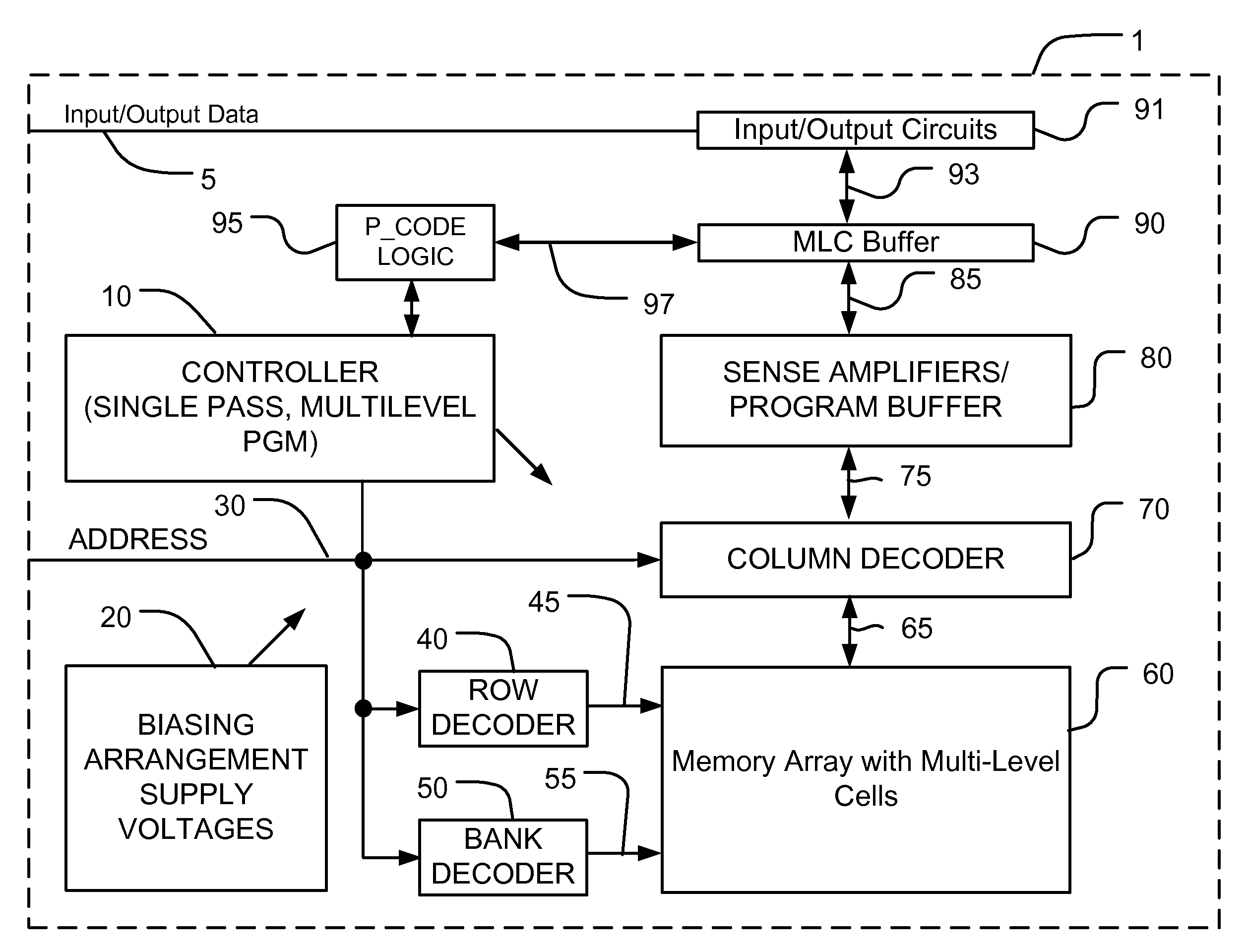
[0045]A detailed description of embodiments is provided with reference to the FIGS. 1-30. FIG. 1 is a simplified chip block diagram of an integrated circuit 1 configured for one-pass, multiple-level programming operations. The integrated circuit 1 includes a memory array 60 including multiple-level cells MLC that store more than one bit of data per cell, on an integrated circuit substrate.

[0046]A row decoder 40 is coupled to a plurality of word lines 45, and arranged along rows in the memory array 60. A bank decoder 50 is coupled to a plurality of bank select lines 55 (such as SSL lines and GSL lines). A column decoder 70 is coupled to a plurality of bit lines 65 arranged along columns in the memory array 60 for reading data from and writing data to the memory array 60. Addresses are supplied on bus 30 from control logic 10 to column decoder 70, and row decoder 40. A sense amplifier and program buffer circuits 80 are coupled to the column decoder 70, in this example via a first data...


PUM


Abstract

A multiple bits per cell memory is operated by applying a one-pass, multiple-level programming, using a single pulse sequence one time (or in one-pass), such as an incremental pulse program sequence, with program verify steps for multiple target program levels, to program multiple bits per cell in a plurality of memory cells. Using these techniques, the number of program pulses required, and the time required for programming the data can be reduced. As a result, an improvement in programming throughput and a reduction in disturbance conditions are achieved. Variants of the one-pass, multiple-level programming operation can be adopted for a variety of memory cell types, memory architectures, programming speeds, and data storage densities.

Description

RELATED APPLICATIONS[0001]This application claims the benefit of U.S. Provisional Patent Application No. 61 / 752,985 filed on 16 Jan. 2013, which application is incorporated by reference as if fully set forth herein.BACKGROUND[0002]1. Field of the Invention[0003]The present invention relates to high density memory devices, and particularly the operation of devices using stacked memory structures.[0004]2. Description of Related Art[0005]As critical dimensions of devices in integrated circuits shrink toward perceived limits of manufacturing technologies, designers have been looking to techniques to achieve greater storage capacity, and to achieve lower costs per bit. Technologies being pursued include storing multiple bits per cell and stacking multiple planes of memory cells on a single chip.[0006]Programming operations for multiple bit per cell technologies can consume significant amounts of time, compared to single bit per cell implementations, because of the requirement to establis...

Claims


Application Information

Patent Timeline
IPC IPC(8): G11C16/10
CPCG11C16/10G11C11/5628G11C16/0483G11C16/3459G11C2211/5621G11C2216/14H01L27/11551H01L27/11578H10B41/20H10B43/20
Inventor HSIEH, CHIH-CHANGCHEN, TI-WENLI, YUNG CHUNCHANG, KUO-PIN
Owner MACRONIX INT CO LTD
Why Eureka
Try Eureka