Circuit and Method for Measuring Delays between Edges of Signals of a Circuit

a delay measurement and circuit technology, applied in the direction of electronic circuit testing, measurement devices, instruments, etc., can solve the problems of significant delay variation, significant jitter, and proportional cost of automatic testing equipment that tests ics

Active Publication Date: 2014-07-24
SIEMENS PROD LIFECYCLE MANAGEMENT SOFTWARE INC
View PDF3 Cites 17 Cited by
  • Summary
  • Abstract
  • Description
  • Claims
  • Application Information

AI Technical Summary

Problems solved by technology

The cost of automatic test equipment that tests ICs is proportional to the number of IC pins to be accessed, and the required measurement accuracy.
Delay circuits on an IC (“on-chip”) have significant jitter caused by power supply noise and significant delay variation caused by temperature and processing variations.

Method used


Image

  • Circuit and Method for Measuring Delays between Edges of Signals of a Circuit
  • Circuit and Method for Measuring Delays between Edges of Signals of a Circuit
  • Circuit and Method for Measuring Delays between Edges of Signals of a Circuit

Examples


Embodiment Construction

[0045]In the following detailed description, numerous specific details are set forth in order to provide a thorough understanding of the present invention. However, it will be understood by those skilled in the art that the present invention may be practiced without these specific details. In other instances, well known methods, procedures, components and circuits have not been described in detail so as not to obscure aspects of the present invention.

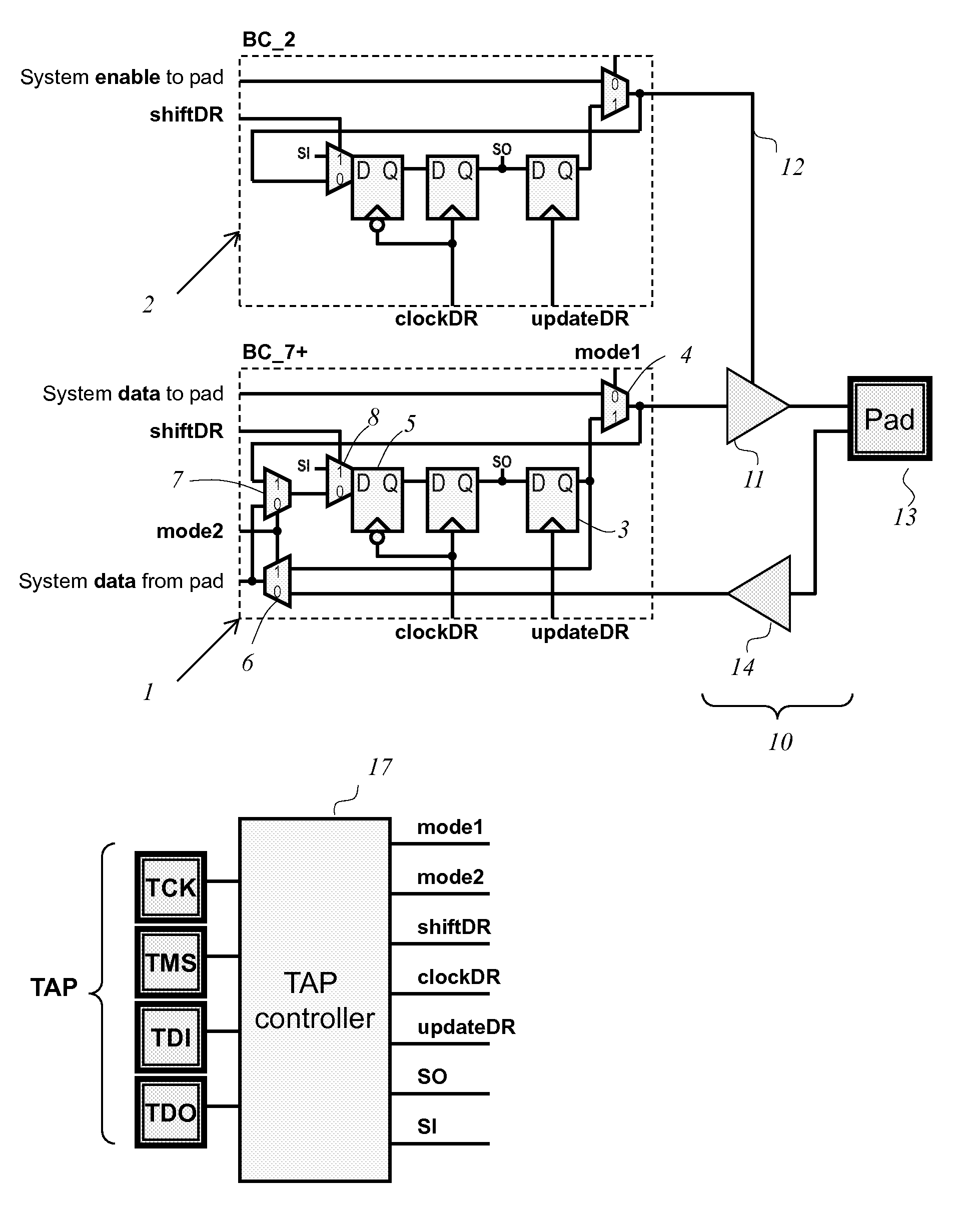
[0046]The circuit of FIG. 1 shows two boundary scan cells, consistent with 1149.1 specifications and connected to pad I / O circuitry of an IC. One cell 1 provides test data to the pad's driver 11 from an update latch 3 connected to a parallel output SO of the BSR, and captures data from the pad's receiver 14 via multiplexer 7 at a parallel input to the BSR, and one cell 2 provides an enable signal 12 to the pad driver.

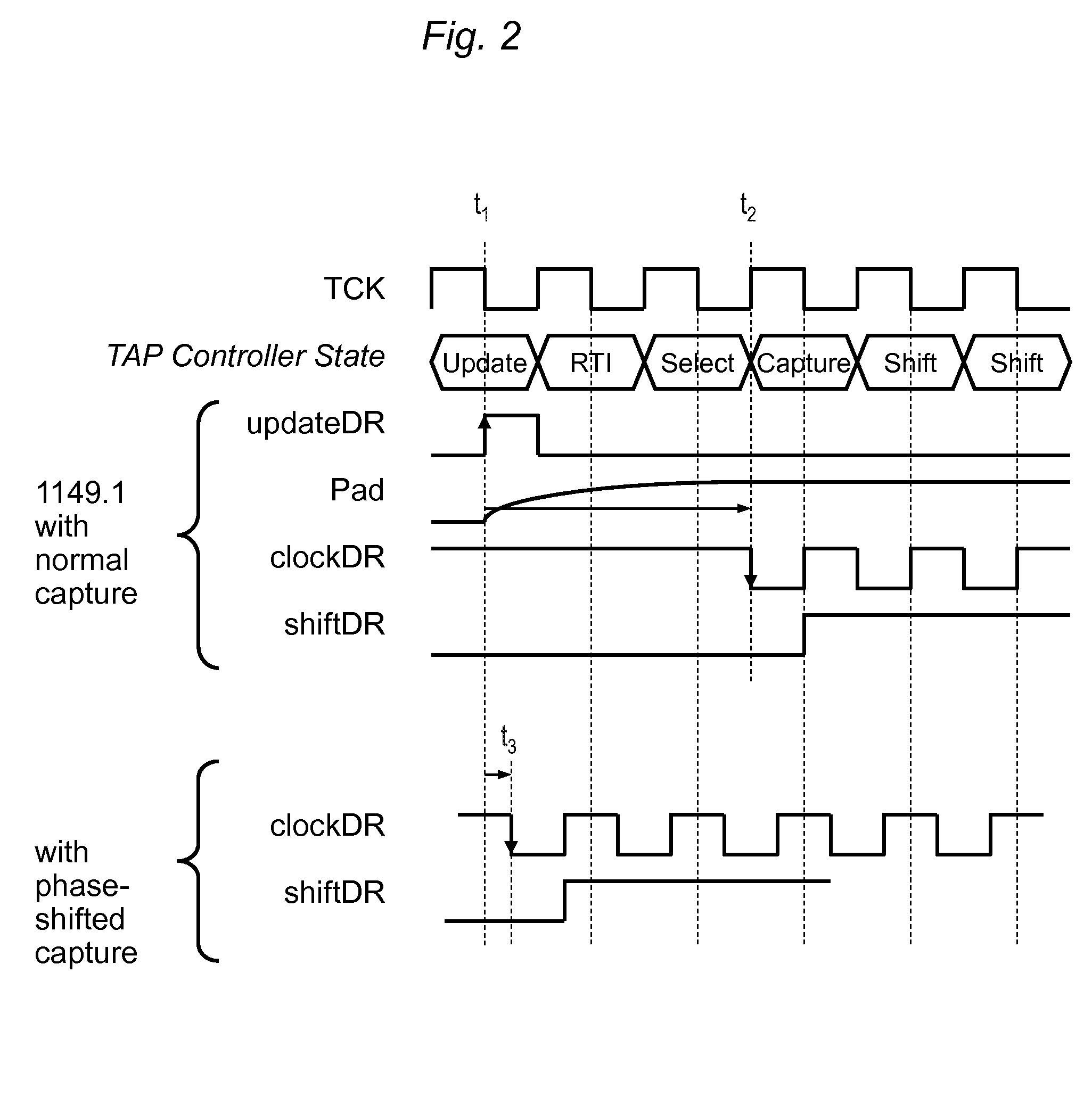
[0047]Consistent with 1149.1, a common TAP controller 17 provides clocks (clockDR and updateDR) and control signals (mode...


PUM


Abstract

Various aspects of the present invention relate to techniques of measuring delays between edges of signals of a circuit. Alternating signals, synchronous to a first clock, are supplied to a plurality of nodes of the circuit. First samples of a plurality of signals associated with the alternating signals are captured using a first capture clock, of which sampling instants are synchronous to a second clock. Second samples of the first samples are then captured using a second capture clock, of which sampling instants are also synchronous to the second clock. The captured second samples are conveyed via a shift register to a plurality of modulo counters. The measured signal delay includes a timing skew associated with the first clock and a timing skew of the first capture clock but not a timing skew of the second capture clock.

Description

RELATED APPLICATIONS[0001]This application is a continuation-in-part application of U.S. application Ser. No. 13 / 941,796, filed on Jul. 15, 2013.[0002]The U.S. application Ser. No. 13 / 941,796 is a divisional application of U.S. application Ser. No. 13 / 018,002, filed on Jan. 31, 2011 and issued as a patent on Jul. 16, 2013 (U.S. Pat. No. 8,489,947).[0003]The U.S. application Ser. No. 13 / 018,002 claims the benefit of U.S. Provisional Patent Application No. 61 / 304,629, filed on Feb. 15, 2010.[0004]All of the above patent / applications are incorporated entirely herein by reference.FIELD OF THE INVENTION[0005]This invention relates to measuring signal propagation delays to characterize and test integrated circuits (ICs) and systems containing ICs.BACKGROUND OF THE INVENTION[0006]A standardized way to provide test access to digital pin signals of an IC is to implement digital boundary scan according to the rules defined in the “IEEE Standard Test Access Port and Boundary-Scan Architecture”...

Claims


Application Information

Patent Timeline
Patent Type & Authority Applications(United States)
IPC IPC(8): G01R31/317G01R31/3177
CPCG01R31/3177G01R31/31725G01R31/318577
Inventor SUNTER, STEPHEN KENNETH
Owner SIEMENS PROD LIFECYCLE MANAGEMENT SOFTWARE INC
Why Eureka
Try Eureka