Track-and-hold circuit with low distortion

a low-distortion, track-and-hold technology, applied in the field of track-and-hold circuits, can solve the problems of adversely affecting the performance of adc and limited high-speed adc, and achieve the effect of reducing frequency-dependent harmonic distortion

Active Publication Date: 2010-08-24
TEXAS INSTR INC
View PDF14 Cites 11 Cited by
  • Summary
  • Abstract
  • Description
  • Claims
  • Application Information

AI Technical Summary

Benefits of technology

[0006]The present invention is a track-and-hold circuit capable of tracking an analog input signal and holding a sampled voltage of the analog input signal at a sampling instant for processing by other circuitry, in response to a track signal that alternates with a hold signal. A first capacitor is provided, having a first terminal connected to a power supply terminal. Tracking circuitry operates when in an on state to apply through a resistor a tracking voltage to a second terminal of the first capacitor that corresponds to the voltage of the analog input signal, by applying the tracking voltage to a first terminal of the resistor, the second terminal of the resistor being connected to the second terminal of the first capacitor. A switch, responsive to the track signal and the hold signal, operates to switch the tracking circuitry to an on state in response to the track signal and to an off state in response to the hold signal, the time of change from the track signal to the hold signal comprising the sampling instant. A second capacitor is provided, having a first terminal connected to the first terminal of the resistor and having a second terminal connected to a power supply terminal. The second capacitor substantially reduces frequency-dependent harmonic distortion.

Problems solved by technology

Generally, the performance of high-speed ADC is limited by the performance of its track-and-hold circuit.
However, prior art track-and-hold circuits still suffer from problems such as harmonic distortion, that adversely affects performance of the ADC.

Method used


Image

  • Track-and-hold circuit with low distortion
  • Track-and-hold circuit with low distortion
  • Track-and-hold circuit with low distortion

Examples


Embodiment Construction

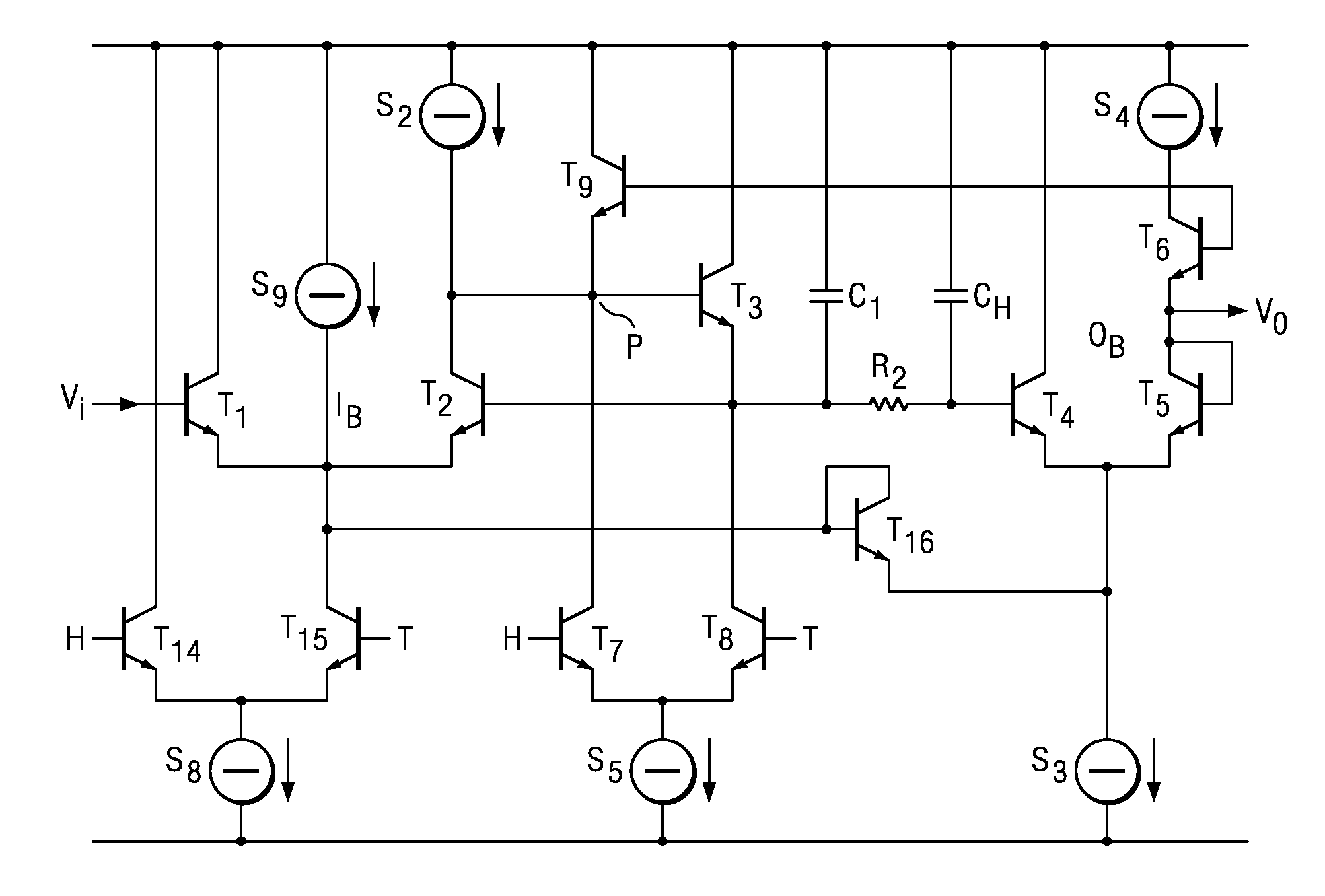
[0015]The making and use of the various embodiments are discussed below in detail. However, it should be appreciated that the present invention provides many applicable inventive concepts which can be embodied in a wide variety of specific contexts. The specific embodiments discussed are merely illustrative of specific ways to make and use the invention, and do not limit the scope of the invention.

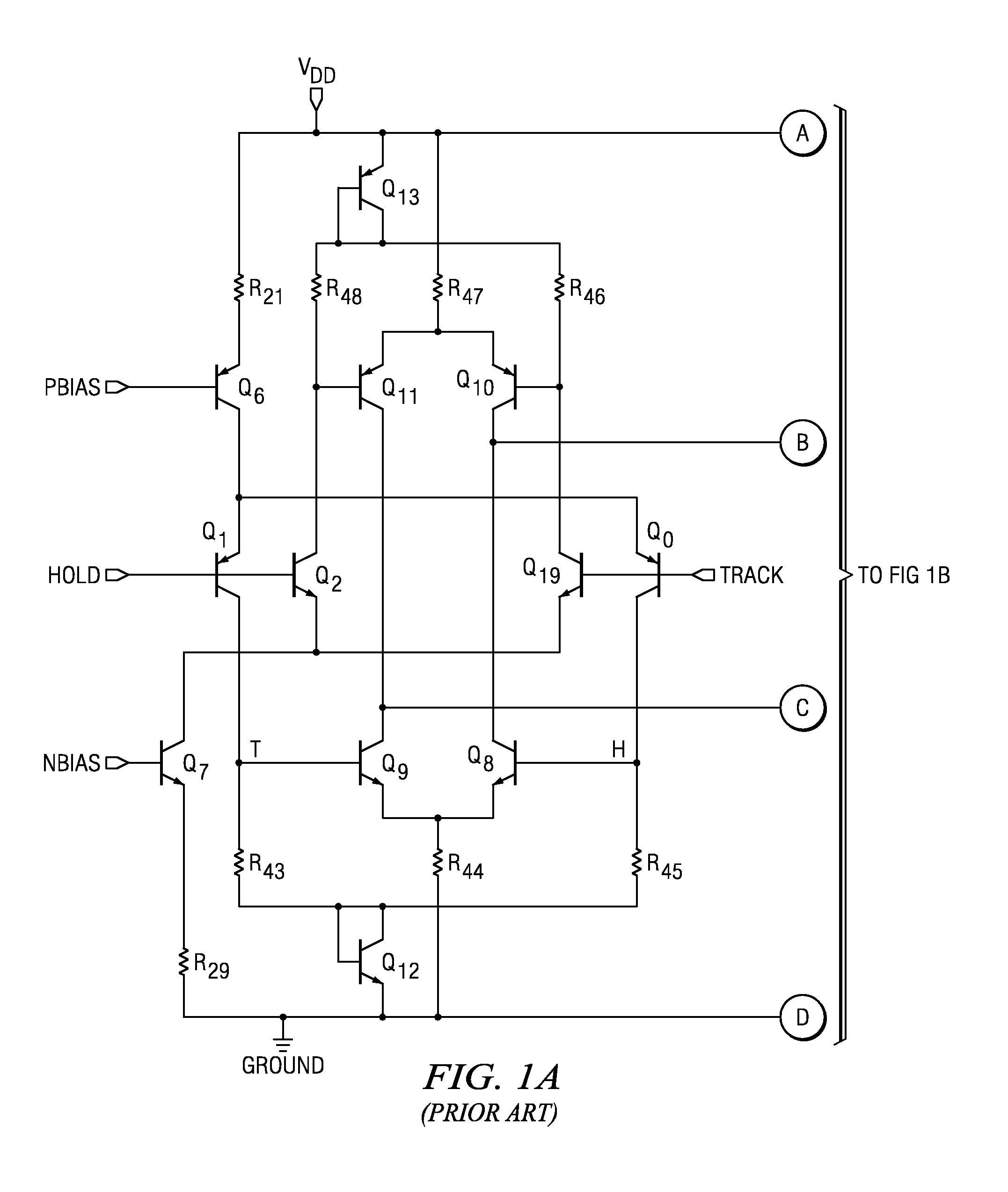
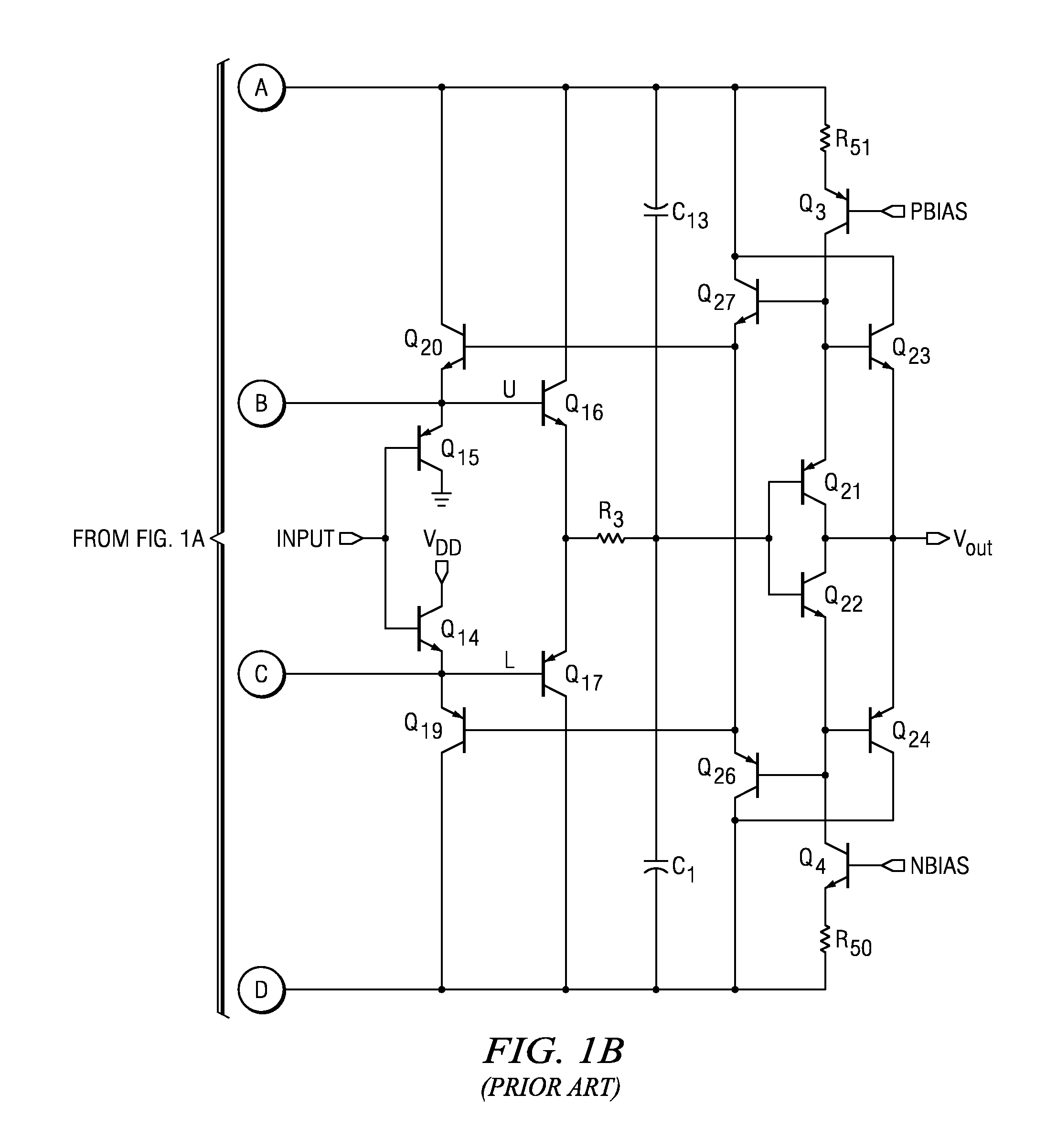
[0016]FIGS. 1A and 1B show a circuit diagram of an example of a prior art sample-and hold circuit. The circuit is powered by a power supply providing a source voltage VDD at a VDD node or terminal, and a current return ground at a GROUND node or terminal. Referring to FIG. 1A, a PNP bipolar transistor Q6 has its emitter connected to VDD through a resistor R21, receiving a positive bias voltage from node PBIAS at its base. The collector of transistor Q6 is connected to the emitter of a PNP bipolar transistor Q1 and to the emitter of a PNP bipolar transistor QO. A diode-connected PNP bipolar...


PUM


Abstract

A track-and-hold circuit capable of tracking an analog input signal and holding a sampled voltage of the analog input signal at a sampling instant for processing by other circuitry, in response to a track signal that alternates with a hold signal. A first capacitor is provided, having a first terminal connected to a power supply terminal. Tracking circuitry operates when in an on state to apply through a resistor a tracking voltage to a second terminal of the first capacitor that corresponds to the voltage of the analog input signal, by applying the tracking voltage to a first terminal of the resistor, the second terminal of the resistor being connected to the second terminal of the first capacitor. A switch, responsive to the track signal and the hold signal, operates to switch the tracking circuitry to an on state in response to the track signal and to an off state in response to the hold signal, the time of change from the track signal to the hold signal comprising the sampling instant. A second capacitor is provided, having a first terminal connected to the first terminal of the resistor and having a second terminal connected to a power supply terminal. The second capacitor substantially reduces frequency-dependent harmonic distortion.

Description

TECHNICAL FIELD OF THE INVENTION[0001]The present invention relates to track and hold circuits, and more particularly relates to a method for improving the performance of such circuits.BACKGROUND OF THE INVENTION[0002]High-speed, low-power analog-to-digital converters (ADCs) are widely used in numerous applications, for example in portable wireless communications devices. The general architecture of a typical ADC is shown in FIG. 3. An analog input signal IA is provided to a track-and-hold (or, sample-and-hold) circuit that receives IA and samples the voltage of that signal at regular intervals. These sample voltages are each held for a period, and provided serially to form an output signal IS that is provided as an output of the track-and-hold circuit and as an input to the following stage, a quantizer. The quantizer converts the values of the voltage levels of IS to a digital signal, that it outputs as OD.[0003]The requirement for ever improved performance in the commercial world ...

Claims


Application Information

Patent Timeline
Patent Type & Authority Patents(United States)
IPC IPC(8): H03K5/00
CPCG11C27/026H03M1/0624H03M1/1245
Inventor CORSI, MARCOPAYNE, ROBERT
Owner TEXAS INSTR INC
Why Eureka
Try Eureka