Radio frequency switch and radio frequency module

a radio frequency module and frequency switch technology, applied in the field of switches, can solve the problems of developing a further insertion loss, more power consumption, and further insertion loss, and achieve the effects of excellent distortion characteristics, small size, and excellent distortion characteristics

Inactive Publication Date: 2012-05-10
PANASONIC CORP
View PDF0 Cites 41 Cited by
  • Summary
  • Abstract
  • Description
  • Claims
  • Application Information

AI Technical Summary

Benefits of technology

[0035]The application of a radio frequency switch according to an implementation of the present invention to a radio frequency amplification module successfully provides a radio frequency module having excellent dis

Problems solved by technology

Increasing the number of stages of the FETs connected in series, as shown in the conventional technique, inevitably develops a further insertion loss when the FETs are conductive.
A greater threshold voltage, however, develops a greater ON-resistance, which results in a further insertion loss when the FETs are conductive.
Accordingly, the gate leakage current inevitably increases, resulting in more power consumption.
Furthermore, in most cases, the maximum voltage t

Method used


Image

  • Radio frequency switch and radio frequency module
  • Radio frequency switch and radio frequency module
  • Radio frequency switch and radio frequency module

Examples


embodiment 1

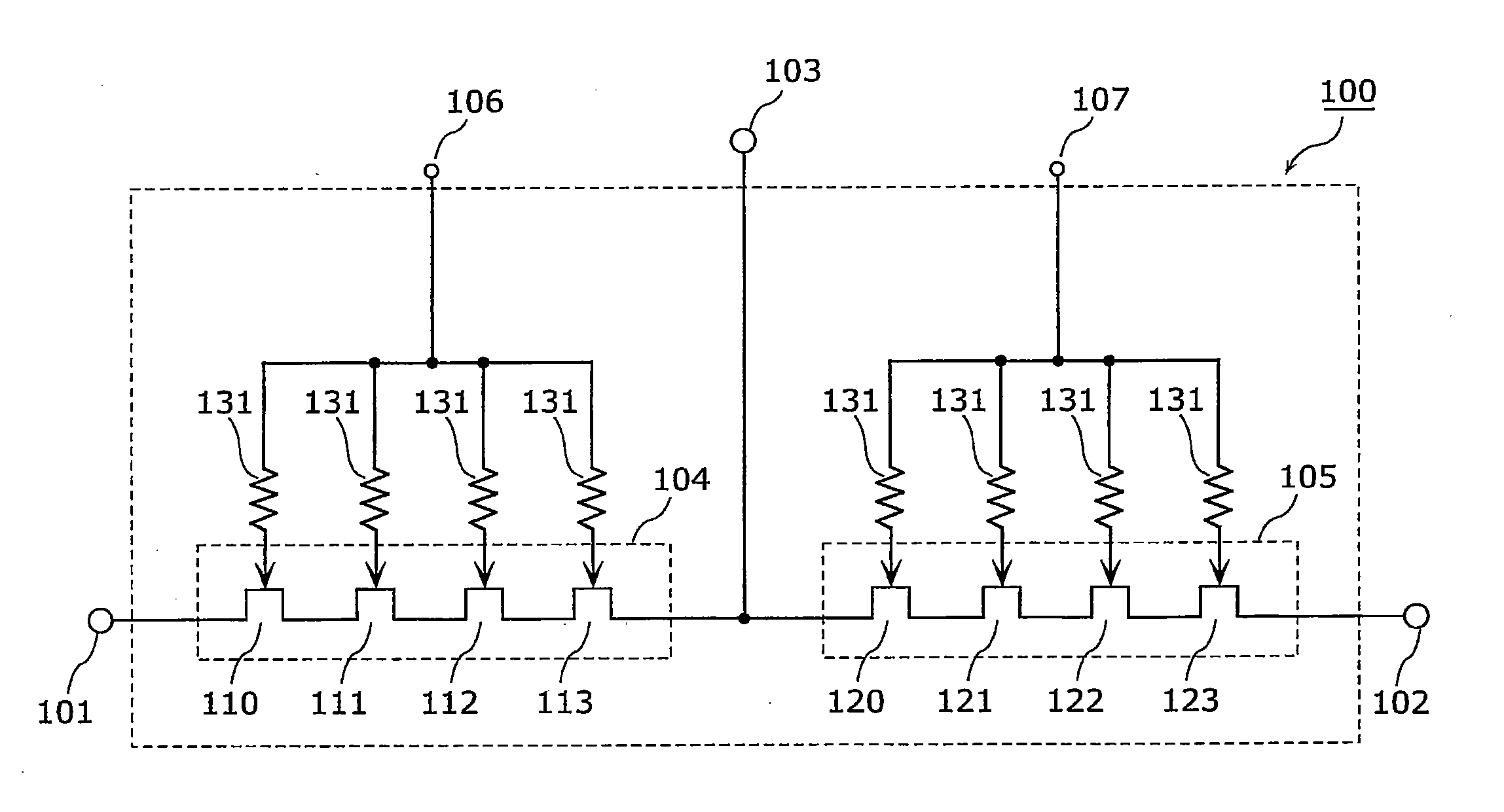
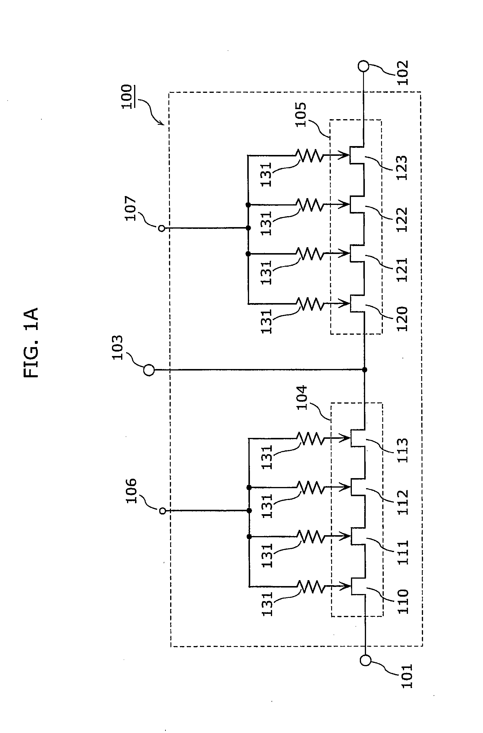
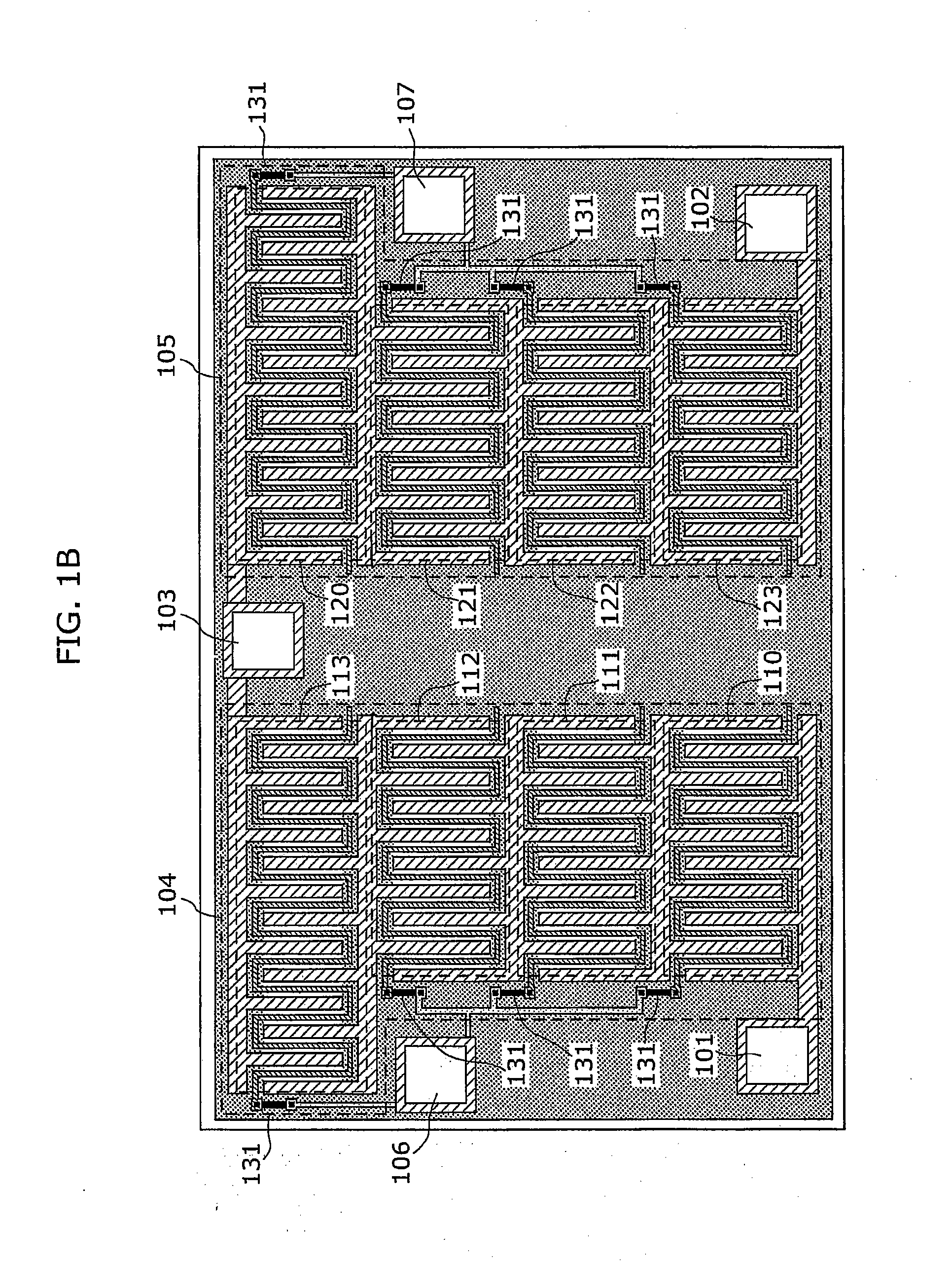
[0054]FIG. 1A shows a circuit diagram of a radio frequency switch according to Embodiment 1 of the present invention. FIG. 1B shows a plan view of the radio frequency switch according to Embodiment 1 of the present invention. A radio frequency switch 100 in FIGS. 1A and 1B includes: input-output terminals 101, 102, and 103; control terminals 106 and 107; a basic switching unit 104 having FETs 110, 111, 112, and 113; and a basic switching unit 105 having FETs 120, 121, 122, and 123. Each of resistive elements 131 has (i) one end connected to a corresponding one of the gate electrodes of the FETs, and (ii) the other end connected to one of the control terminals 106 and 107.

[0055]Embodiment 1 is characterized as follows: Among the FETs included in the radio frequency switch, the finger lengths of the FETs 113 and 120 connected to the input-output terminal 103 are shorter than the finger lengths of the rest of the FETs.

[0056]The radio frequency switch 100 shown in FIGS. 1A and 1B works ...

embodiment 2

[0073]Embodiment 2 mainly describes the points which differ from those in Embodiment 1. Configurations, operations, and effects similar to those in Embodiment 1 shall be omitted.

[0074]FIG. 5 shows a circuit diagram of a radio frequency switch according to Embodiment 2 of the present invention. The radio frequency switch 500 in FIG. 5 includes: the input-output terminals 101, 102, and 103; the control terminals 106 and 107; a basic switching unit 504 having FETs 510, 511, 512, and 513; a basic switching unit 505 having FETs 520, 521, 522, and 523; a basic switching unit 506 having FETs 530, 531, 532, and 533; and a basic switching unit 507 having FETs 540, 541, 542, and 543. Each of electric potential fixed resistors 550 has one end and the other end respectively connected to the source electrode and to the drain electrode of a corresponding FET in order to fix a DC potential of the corresponding FET.

[0075]Embodiment 2 is characterized in that, among the FETs included in the radio fr...

embodiment 3

[0086]Embodiment 3 mainly describes the points which differ from those in Embodiment 1. Configurations, operations, and effects similar to those in Embodiment 1 shall be omitted.

[0087]FIG. 6 shows a circuit diagram of a radio frequency switch according to Embodiment 3 of the present invention. A radio frequency switch 600 in FIG. 6 includes: the input-output terminals 101, 102, and 103; the second control terminals 106 and 107; a basic switching unit 604 having FETs 610 and 611; and a basic switching unit 605 having FETs 620 and 621.

[0088]Embodiment 3 is characterized in that the FETs included in the radio frequency switch 600 are multi-gate FETs. A multi-gate FET has at least two gate electrodes between the source electrode and the drain electrode. The radio frequency switch 600 in FIG. 6 works as an SPDT switch circuit.

[0089]The input-output terminals 101 to 103 are used for inputting and outputting radio frequency signals. For example, the input-output terminal 101 connects to a ...


PUM


Abstract

The present invention provides a radio frequency switch and a radio frequency module having excellent distortion characteristics without causing a further insertion loss and a greater chip size. The radio frequency switch includes: input-output terminals which are for inputting and outputting a radio frequency signal; a basic switching unit provided between two of the input-output terminals; and a control terminal which receives a control voltage for controlling conduction and interruption of the basic switching unit. The basic switching unit includes field effect transistors (FETs) connected in multiple stages, each of the FETs being a meandered FET having a meandered gate electrode, and among the FETs, one of the FETs has a finger length shorter than finger lengths of rest of the FETs, the one of the FETs electrically located closest to one of the input-output terminals.

Description

BACKGROUND OF THE INVENTION[0001](1) Field of the Invention[0002]The present invention relates to switches for controlling conduction and interruption by a field effect transistor (FET) and, more particularly, to a radio frequency switch which intermittently transmits a radio frequency signal, and to a radio frequency module including the radio frequency switch.[0003](2) Description of the Related Art[0004]Most of mobile communications devices, such as cellular phones, are typically configured to use one antenna for both transmission and reception so that the devices can be made smaller. In such a configuration, it is necessary to switch internal circuits connected to the antenna depending on whether the signals are transmitted or received, and a radio frequency signal switch is used for the switching. Furthermore, not only the connection with the antenna, the radio frequency switch is used when switching radio frequency signal paths in the circuits according to the communication sc...

Claims


Application Information

Patent Timeline
IPC IPC(8): H03F3/68H03K17/687
CPCH03F3/72H03F2200/111H03F2200/451H03K17/102H03F2203/7236H03K17/693H03F2203/7209
Inventor KAWANO, HIROAKIKOIZUMI, HARUHIKOWAKITA, KAZUYA
Owner PANASONIC CORP
Why Eureka
Try Eureka