
Methods for fabricating integrated circuits having confined epitaxial growth regions

a technology of epitaxial growth and integrated circuit, which is applied in the direction of basic electric elements, electrical equipment, semiconductor devices, etc., can solve the problems of reducing mobility, reducing carrier lifetime, and crystalline defects in growing materials, so as to achieve higher chemical bond energy and reduce reactivity

Active Publication Date: 2014-07-31
GLOBALFOUNDRIES US INC
View PDF2 Cites 77 Cited by
  • Summary
  • Abstract
  • Description
  • Claims
  • Application Information

AI Technical Summary

Benefits of technology

This patent text describes methods for making integrated circuits using semiconductor materials. One method involves forming a confinement isolation material on a semiconductor substrate and then adding a liner dielectric material over the isolation material to passivate its surface. An epitaxial layer of semiconductor material is then grown on top of the semiconductor substrate. Another method involves forming semiconductor fins on a semiconductor substrate and adding a liner dielectric material and an isolation oxide to fill the spaces between the fins. The top surface of the fins and a portion of the liner dielectric layer are then exposed and treated with a silane coupling agent. A crystalline semiconductor material is then epitaxially grown on the exposed fins, and the isolation oxide and liner dielectric layer are etched to expose a side portion of the epitaxial material. These methods may provide improved performance and reliability for integrated circuits.

Problems solved by technology

A crystalline mismatch at the interface between the confinement isolation material and the growing epitaxial material can cause the formation of crystalline defects in the growing material.
Such defects can reduce mobility, reduce carrier lifetime, and increase leakage in devices formed in and on the grown material.

Method used


Image

  • Methods for fabricating integrated circuits having confined epitaxial growth regions
  • Methods for fabricating integrated circuits having confined epitaxial growth regions
  • Methods for fabricating integrated circuits having confined epitaxial growth regions

Examples


Embodiment Construction

[0010]The following detailed description is merely exemplary in nature and is not intended to limit the various embodiments or the application and uses thereof. Furthermore, there is no intention to be bound by any expressed or implied theory presented in the preceding technical field, background, brief summary or the following detailed description.

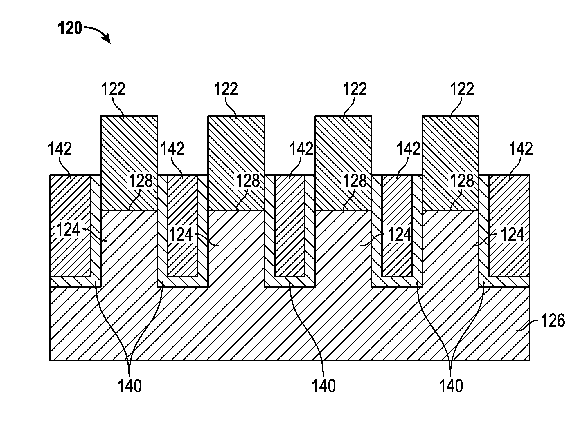
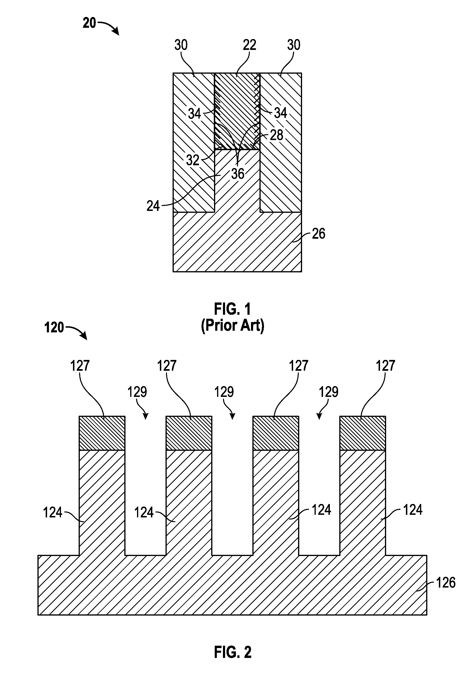
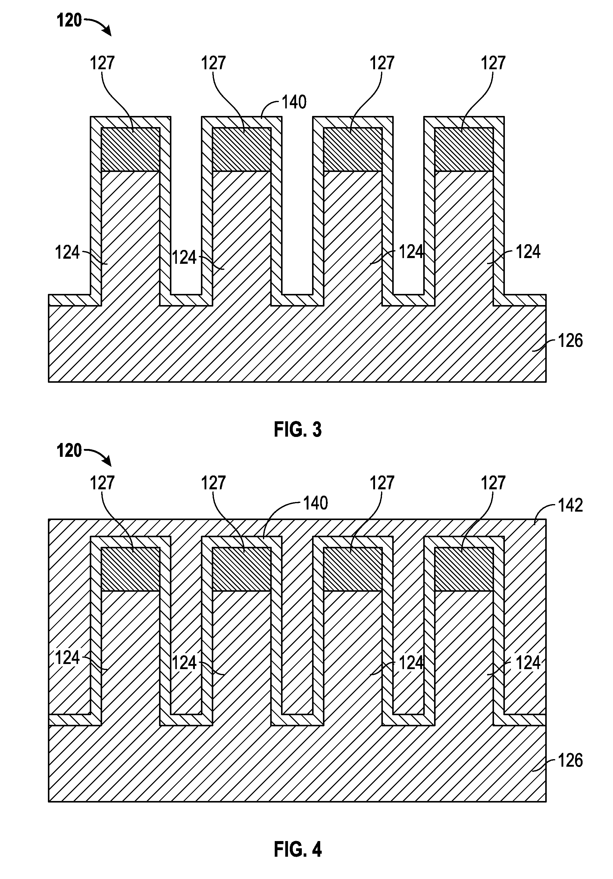
[0011]Confined epitaxial growth finds application in the fabrication of various semiconductor integrated circuits (ICs). For example, confined epitaxial growth can be used in the fabrication of FinFETs in which the epitaxial material is grown on the top of semiconductor fins to provide a desired material for the channel of the FinFET as well as for the source and drain regions. The epitaxially grown material can be either the same as the underlying semiconductor substrate, or can be different material as required to provide the desired mobility or other characteristic needed for the IC being fabricated. For example, if the semiconductor s...


PUM


Abstract

Methods are provided for fabricating integrated circuits. In accordance with one embodiment, the method includes forming a portion of a semiconductor substrate at least partially bounded by a confinement isolation material. A liner dielectric is formed overlying the confinement isolation material and is treated to passivate a surface thereof An epitaxial layer of semiconductor material is then grown overlying the portion of semiconductor substrate.

Description

TECHNICAL FIELD[0001]The technical field generally relates to methods for fabricating integrated circuits, and more particularly relates to methods for fabricating integrated circuits with reduced sidewall-formed defects in confined epitaxial growth.BACKGROUND[0002]Confined epitaxial growth is used in the fabrication of many different types of integrated circuits. For example, confined epitaxial growth is used to improve the mobility characteristics of the channel region of non-planar field effect transistors (FETs) such as FinFETs. Confined epitaxial growth is also used to impart a strain on the channel region, and hence to increase the mobility, of planar FETs. In each of these examples, as well as in other applications of confined epitaxial growth, the epitaxial growth is nucleated on a portion of monocrystalline substrate that is, at least, partially bounded by a non-crystalline confinement isolation material. A crystalline mismatch at the interface between the confinement isola...

Claims


Application Information

Patent Timeline
IPC IPC(8): H01L21/762
CPCH01L21/76224H01L21/02532H01L21/0262H01L21/02658H01L21/3105H01L29/66795
Inventor LICAUSI, NICHOLASFRONHEISER, JODYRYAN, ERROL TODD
Owner GLOBALFOUNDRIES US INC
Features
  • Generate Ideas
  • Intellectual Property
  • Life Sciences
  • Materials
  • Tech Scout
  • Unparalleled Data Quality
  • Higher Quality Content
  • 60% Fewer Hallucinations
Learn More