Magnetic sensor integrated in a chip for detecting magnetic fields perpendicular to the chip and manufacturing process thereof

a technology of magnetic sensors and chip bodies, applied in the direction of magnetic sensor geometrical arrangements, instruments, solid-state devices, etc., can solve the problems of high manufacturing cost, difficult assembly and calibration operations, and difficult production of magnetic sensors sensitive to magnetic fields perpendicular to the surface of chips,

Active Publication Date: 2014-08-07
STMICROELECTRONICS INT NV
View PDF4 Cites 14 Cited by
  • Summary
  • Abstract
  • Description
  • Claims
  • Application Information

AI Technical Summary

Problems solved by technology

On the other hand, production of magnetic sensors sensitive to magnetic fields perpendicular to the surface of a chip (for example, for electronic compasses) is problematic.
However, in this case, the assembly and calibration operations are complex, and the finished device is costly.
In addition, the packaged device has a large volume (in particular, in height), which does not enable use thereof in small apparatuses.
In fact, the presence of horizontal portions (parallel to the chip surface) or portions having a horizontal component causes a deformation of the magnetic field directed parallel to this portion, and thus reading errors.
Moreover, the distance between the concentrator and the Hall sensor determines in any case a loss of field lines of the concentrated field in the area between the concentrator and the Hall sensor, loss that cannot be eliminated since the ferromagnetic material may be a source of silicon contamination and may alter operation of the Hall-effect cell.

Method used


Image

  • Magnetic sensor integrated in a chip for detecting magnetic fields perpendicular to the chip and manufacturing process thereof
  • Magnetic sensor integrated in a chip for detecting magnetic fields perpendicular to the chip and manufacturing process thereof
  • Magnetic sensor integrated in a chip for detecting magnetic fields perpendicular to the chip and manufacturing process thereof

Examples


Embodiment Construction

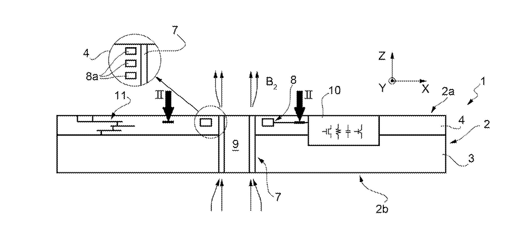
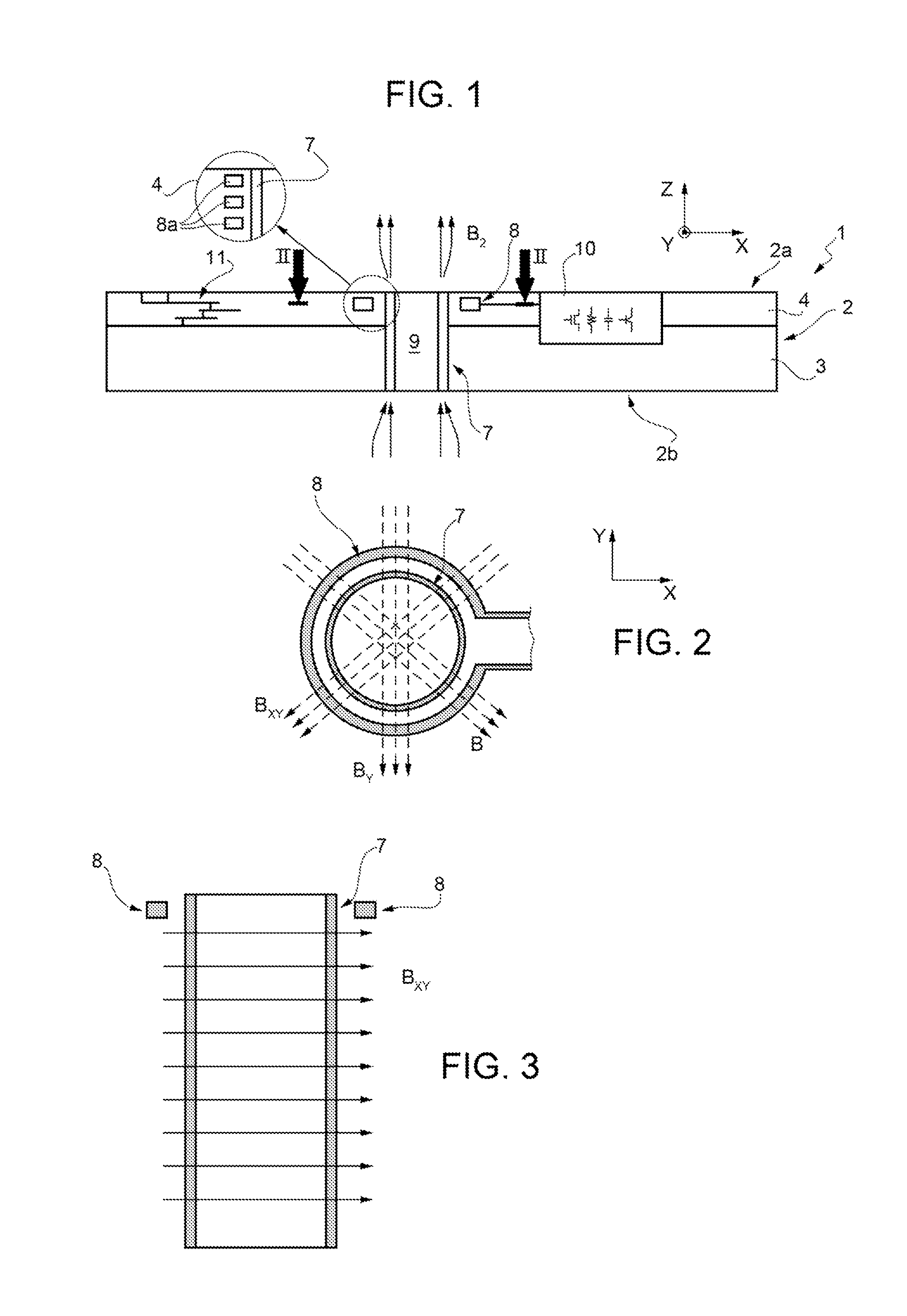
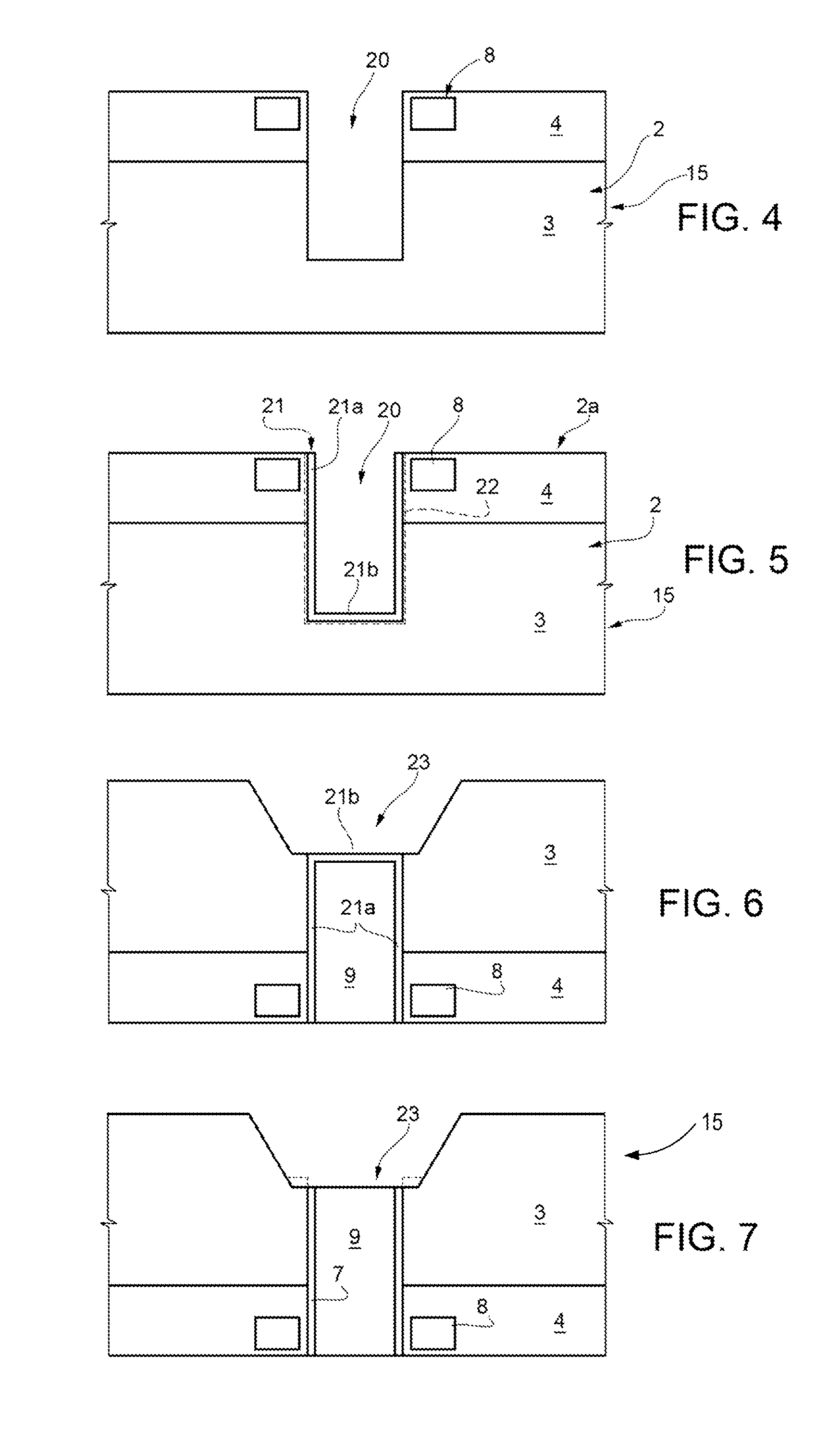
[0017]FIG. 1 shows a magnetic sensor 1 integrated in a chip 2 of semiconductor material, comprising a body 3 and an insulating layer 4 overlying the body 3. In a known manner, not shown, the body 3, for example of silicon, may in turn be formed by a substrate and by one or more epitaxial layers, and the insulating layer 4 may be formed by a plurality of dielectric layers. A plurality of metallization levels are interconnected by conductive vias inside the insulating layer. In a Cartesian reference system XYZ, the chip 2 has a first surface 2a and a second surface 2b (here a top surface, defined by the insulating layer 4, and a rear surface, defined by the body 3), which are parallel to a plane XY, and a thickness measured along an axis Z.

[0018]The magnetic sensor 1 comprises a magnetic via 7, formed by a cylinder of magnetic material, and a sensing coil 8, surrounding at a distance the magnetic via 7 and approximately coaxial thereto. The magnetic via 7 extends perpendicular to the ...


PUM


Abstract

An integrated magnetic sensor formed by a semiconductor chip having a surface and accommodating a magnetic via and a sensing coil. The magnetic via is formed by a cylindrical layer of ferromagnetic material that extends perpendicular to the surface of the first chip and has in cross-section an annular shape of a circular or elliptical or curvilinear type. The sensing coil surrounds the magnetic via at a distance and is connected to an electronic circuit.

Description

BACKGROUND[0001]1. Technical Field[0002]The present disclosure relates to a magnetic sensor integrated in a chip for detecting magnetic fields perpendicular to the chip and to the manufacturing process thereof.[0003]2. Description of the Related Art[0004]Various sensors are known that are able to detect magnetic fields parallel to the surface of a chip integrating the sensor. On the other hand, production of magnetic sensors sensitive to magnetic fields perpendicular to the surface of a chip (for example, for electronic compasses) is problematic. In fact, integrated magnetic sensors currently available on the market are substantially sensitive to fields directed parallel to the plane of the sensor (plane XY), and a sensor that is sensitive along the axis Z is obtained by arranging the chip of the corresponding sensor in a direction perpendicular to the chips of the X and Y sensors. However, in this case, the assembly and calibration operations are complex, and the finished device is...

Claims


Application Information

Patent Timeline
Patent Type & Authority Applications(United States)
IPC IPC(8): H01L43/02
CPCH01L43/02G01R33/0005G01R33/0011G01R33/0047G01R33/04H01L2224/48091H01L2224/48227H01L2924/15311H01L2224/16227H01L2924/18161H01L2924/00014H01L2224/16225H01L2224/05571H01L2224/05573H10N50/80H01L2224/13099H01L2224/05599
Inventor PAGANI, ALBERTO
Owner STMICROELECTRONICS INT NV
Why Eureka
Try Eureka