Non-planar gate all-around device and method of fabrication thereof

a technology of all-around devices and non-planar gates, which is applied in the direction of semiconductor devices, electrical devices, nanotechnology, etc., can solve the problems of problematic tunneling paths between source and drain, and achieve the effect of reducing the risk of leakag

Active Publication Date: 2014-08-14
SONY CORP
View PDF1 Cites 611 Cited by
  • Summary
  • Abstract
  • Description
  • Claims
  • Application Information

AI Technical Summary

Problems solved by technology

Unfortunately, the fourth side, the bottom part of the channel is far away from the gate electrode and thus is not under close gate control.
As transistor dimensions are continually scaled down to sub 20-25 nm technology nodes, parasitic leakage paths between the source and drains become problematic for tri-gate transistors.

Method used


Image

  • Non-planar gate all-around device and method of fabrication thereof
  • Non-planar gate all-around device and method of fabrication thereof
  • Non-planar gate all-around device and method of fabrication thereof

Examples


Embodiment Construction

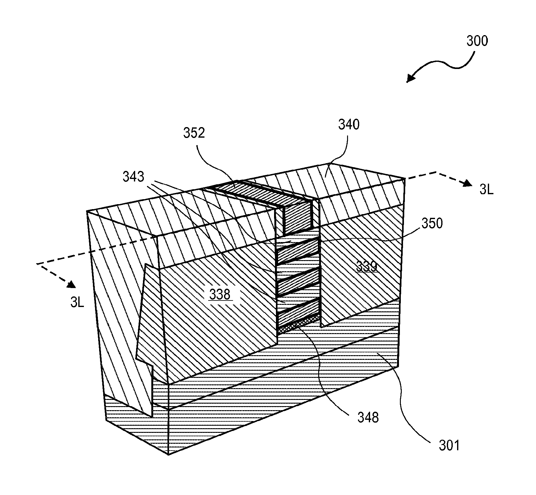
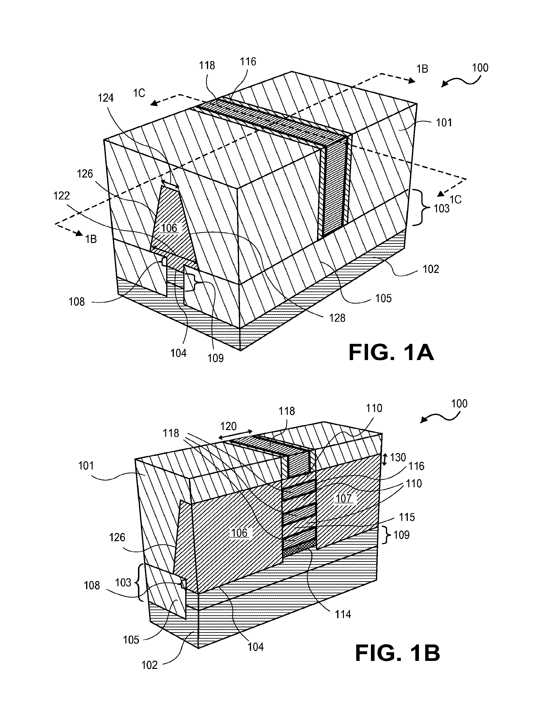
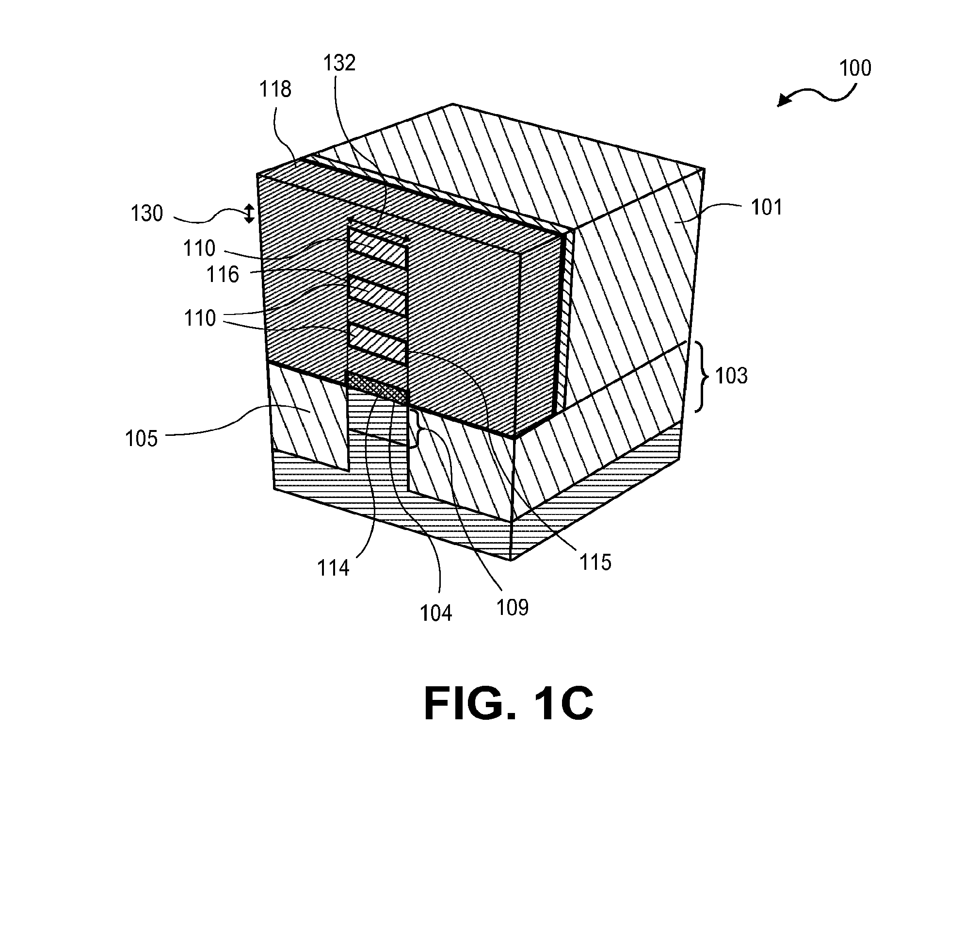
[0012]The present invention is a novel gate all-around transistor and a method of fabrication. In the following description, numerous details are set forth in order to provide a thorough understanding of the present invention. It will be apparent, however, to one skilled in the art, that the present invention may be practiced without these specific details. In other instances, well-known semiconductor processes and manufacturing techniques have not been described in detail to avoid obscuring the present invention. Reference throughout this specification to “an embodiment” means that a particular feature, structure, function, or characteristic described in connection with the embodiment is included in at least one embodiment of the invention. Thus, the appearances of the phrase “in an embodiment” in various places throughout this specification are not necessarily referring to the same embodiment of the invention. Furthermore, the particular features, structures, functions, or charact...


PUM


Abstract

A non-planar gate all-around device and method of fabrication thereby are described. In one embodiment, the device includes a substrate having a top surface with a first lattice constant. Embedded epi source and drain regions are formed on the top surface of the substrate. The embedded epi source and drain regions have a second lattice constant that is different from the first lattice constant. Channel nanowires having a third lattice are formed between and are coupled to the embedded epi source and drain regions. In an embodiment, the second lattice constant and the third lattice constant are different from the first lattice constant. The channel nanowires include a bottom-most channel nanowire and a bottom gate isolation is formed on the top surface of the substrate under the bottom-most channel nanowire. A gate dielectric layer is formed on and all-around each channel nanowire. A gate electrode is formed on the gate dielectric layer and surrounding each channel nanowire.

Description

BACKGROUND[0001]1) Field[0002]Embodiments of this invention relate to the field of semiconductor devices and more particularly to a non-planar gate all-around device and method of fabrication.[0003]2) Description of Related Art[0004]As integrated device manufacturers continue to shrink the feature sizes of transistor devices to achieve greater circuit density and higher performance, there is a need to enhance transistor drive currents while reducing short-channel effects such as parasitic capacitance and off-state leakage for next-generation devices. One way of increasing transistor drive currents is to use higher carrier mobility semiconductor materials to form the channel. Higher carrier mobility in the channel supports higher transistor drive currents. Carrier mobility is a measure of the velocity at which carriers flow in a semiconductor material under an external unit electric field. Process induced stress (sometimes referred to as stress) on the semiconductor body is another w...

Claims


Application Information

Patent Timeline
Patent Type & Authority Applications(United States)
IPC IPC(8): H01L29/06H01L29/78H01L29/66
CPCH01L29/42392H01L29/785H01L29/7848H01L29/165H01L29/66795H01L29/78696H01L29/0669H01L29/0673H01L29/7851H01L29/045H01L29/1033H01L2029/7858B82Y10/00H01L29/66439H01L29/775H01L29/1079H01L29/7842H01L29/78618
Inventor RACHMADY, WILLYPILLARISETTY, RAVILE, VAN H.KAVALIEROS, JACK T.CHAU, ROBERT S.KACHIAN, JESSICA S.
Owner SONY CORP
Why Eureka
Try Eureka