Light-emitting device

a technology of light-emitting devices and light-emitting tubes, which is applied in the direction of semiconductor devices, basic electric elements, electrical apparatus, etc., can solve the problems of large current flow, crosstalk phenomenon, and deterioration of organic el elements, so as to prevent the occurrence of crosstalk phenomenon

Active Publication Date: 2014-08-14
SEMICON ENERGY LAB CO LTD +1
View PDF5 Cites 9 Cited by
  • Summary
  • Abstract
  • Description
  • Claims
  • Application Information

AI Technical Summary

Benefits of technology

[0033]With one embodiment of the present invention...

Problems solved by technology

However, a large current flow accelerates deterioration of organic EL elements.
One problem of a light-emitting panel in which tandem elements are provided adjacently is occurrence of a crosstalk pheno...

Method used


Image

  • Light-emitting device
  • Light-emitting device
  • Light-emitting device

Examples


embodiment 1

Display Panel Structure

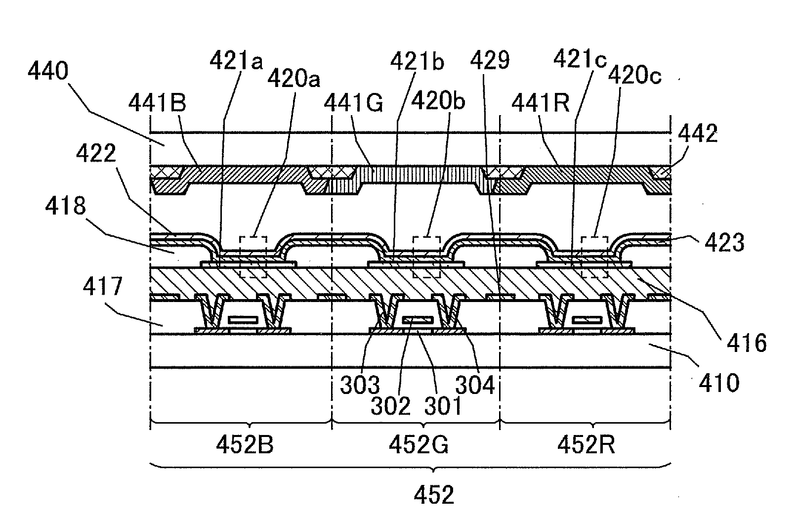
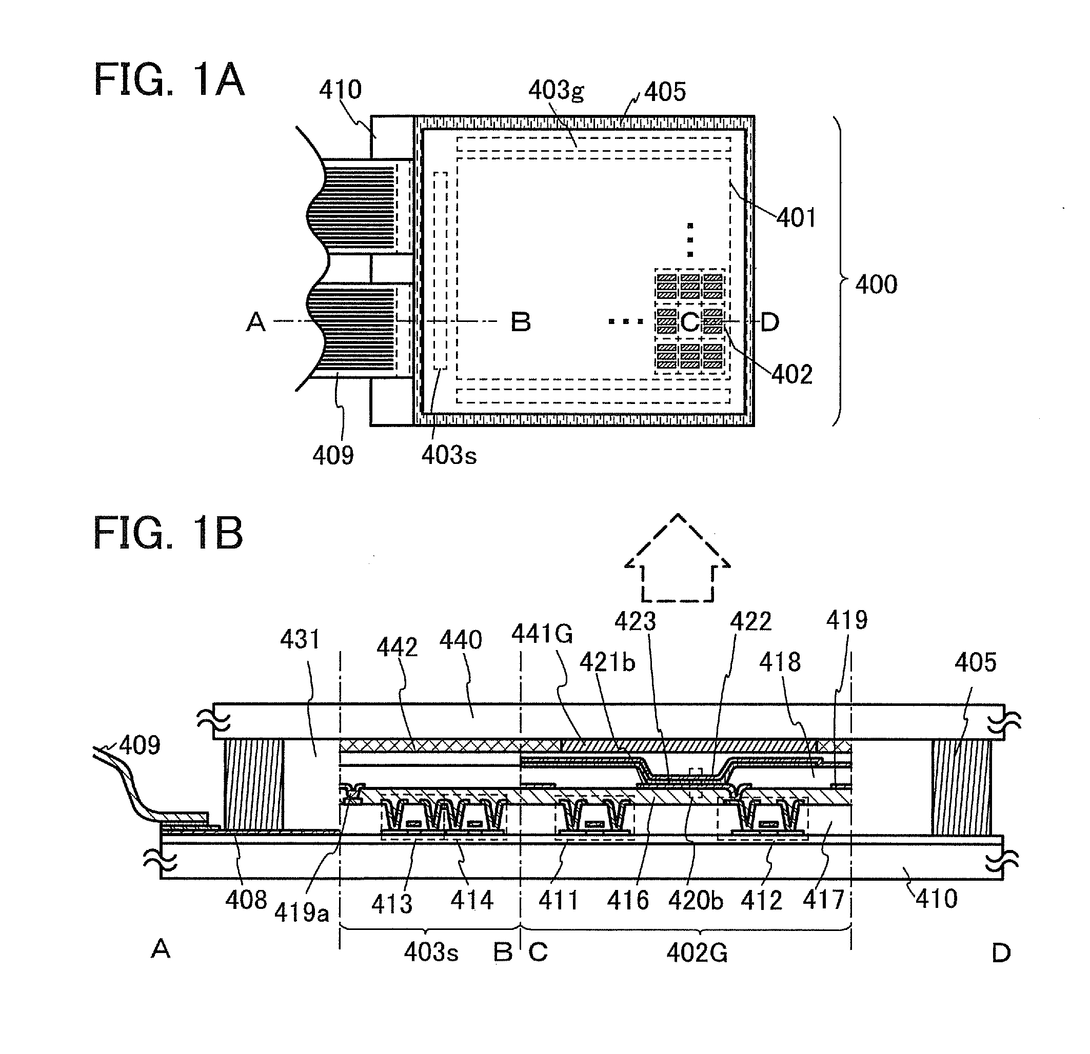
[0043]FIGS. 1A and 1B illustrate a structure of a display panel that can be used for a display device of one embodiment of the present invention. FIG. 1A is a top view of the structure of the display panel which can be used for a display device of one embodiment of the present invention, and FIG. 1B is a side view illustrating the cross section of the structure along section lines A-B and C-D in FIG. 1A.

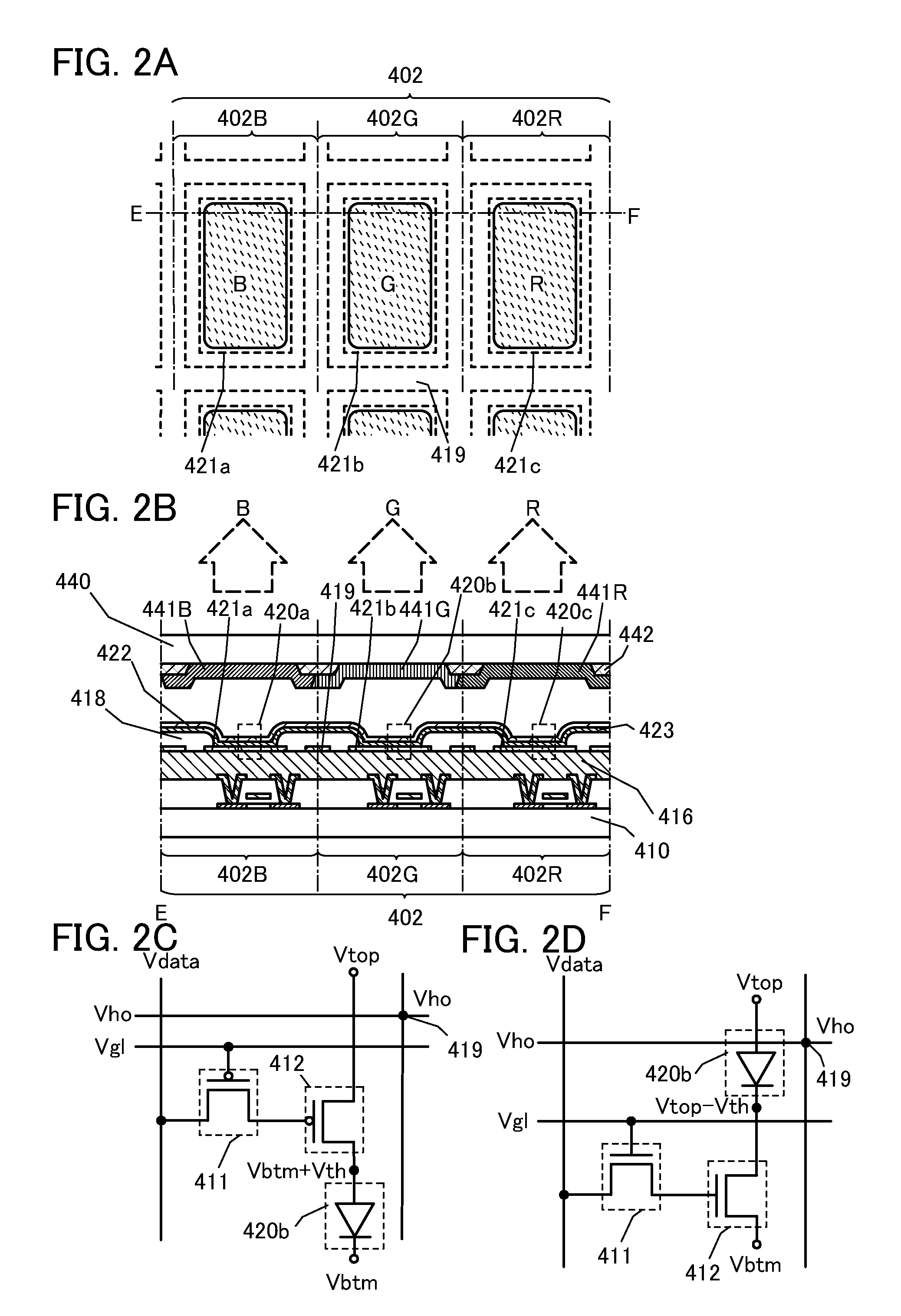
[0044]A display panel 400 shown as an example in this embodiment includes a display portion 401 over a first substrate 410. The display portion 401 includes a plurality of pixels 402. The pixel 402 includes a plurality of sub-pixels (e.g., three sub-pixels) (see FIG. 1A). Over the first substrate 410, in addition to the display portion 401, a source side driver circuit portion 403s and a gate side driver circuit portion 403g which drive the display portion 401 are provided. Note that the driver circuit portions can be provided not over the first substrate 410 b...

example

[0103]In Example, a display panel of one embodiment of the present invention in which a shield electrode is provided between sub-pixels was fabricated, and the presence or absence of crosstalk was checked.

[0104]FIGS. 6A to 6C are enlarged views illustrating a pixel portion of the display panel fabricated in Example. FIG. 6A is a plan view of the pixel portion of the display panel. FIG. 6B is a cross-sectional view along G-H in FIG. 6A. FIG. 6C is an equivalent circuit diagram illustrating a sub-pixel 572B.

[0105]Note that in FIG. 6A, some components (e.g., an upper electrode 556, an EL layer 523, and a partition 518) are omitted in order to clearly show positions of a first lower electrode 554a functioning as a pixel electrode, and a first shield electrode 549a formed using the same layer as the first lower electrode 554a. In FIG. 6A, dotted lines in first, second, and third lower electrodes 554a, 554b, and 554c denote opening portions of the pixel.

[0106]The pixel 572 of the display ...


PUM


Abstract

Occurrence of a crosstalk phenomenon in a light-emitting device is inhibited. A light-emitting device including an insulating layer 416; a first lower electrode 421a formed over the insulating layer; a second lower electrode 421b formed over the insulating layer; a partition 418 formed over the insulating layer and positioned between the first lower electrode and the second lower electrode; a stacked-layer film 423 which is formed over the first lower electrode, the partition, and the second lower electrode and includes a light-emitting layer containing a light-emitting substance and a layer having higher conductivity than that of the light-emitting layer; an upper electrode 422 formed over the stacked-layer film; and a shield electrode 419 which is formed under the partition and does not overlap with the first lower electrode and the second lower electrode.

Description

BACKGROUND OF THE INVENTION[0001]1. Field of the Invention[0002]The present invention relates to a light-emitting device that has a light-emitting element.[0003]2. Description of the Related Art[0004]Commercialization of organic EL displays is accelerating. The required luminance of displays is becoming higher year by year for outdoor use. It is known that the luminance of an organic EL element increases in proportion to electric current, and light emission at high luminance can be achieved.[0005]However, a large current flow accelerates deterioration of organic EL elements. Thus, if high luminance can be achieved with a small amount of current, light-emitting elements can have longer lifetimes. In this regard, a tandem element in which a plurality of light-emitting units is stacked has been proposed as a light-emitting element capable of providing high luminance with a small amount of current (see Patent Document 1, for example).[0006]Note that in this specification, a light-emitti...

Claims


Application Information

Patent Timeline
IPC IPC(8): H01L33/36
CPCH01L27/3241H10K59/131H10K50/852H10K59/805H10K50/805
Inventor NISHIDO, YUSUKEHIRAKATA, YOSHIHARUYAMANAKA, SHIGETSUGU
Owner SEMICON ENERGY LAB CO LTD
Why Eureka
Try Eureka