Inverter device
- Summary
- Abstract
- Description
- Claims
- Application Information
AI Technical Summary
Benefits of technology
Problems solved by technology
Method used
Image
Examples
embodiment 1
Preferred Embodiment 1
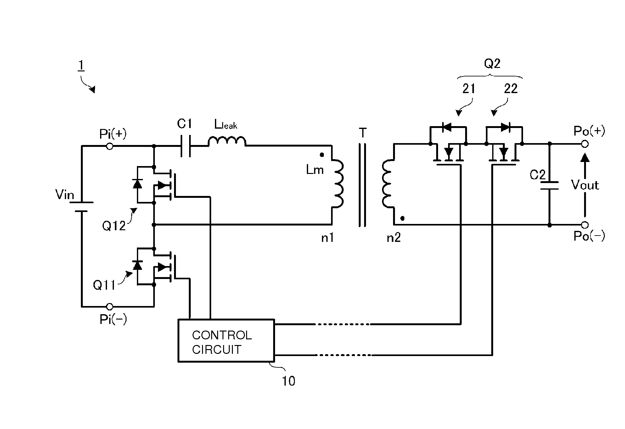
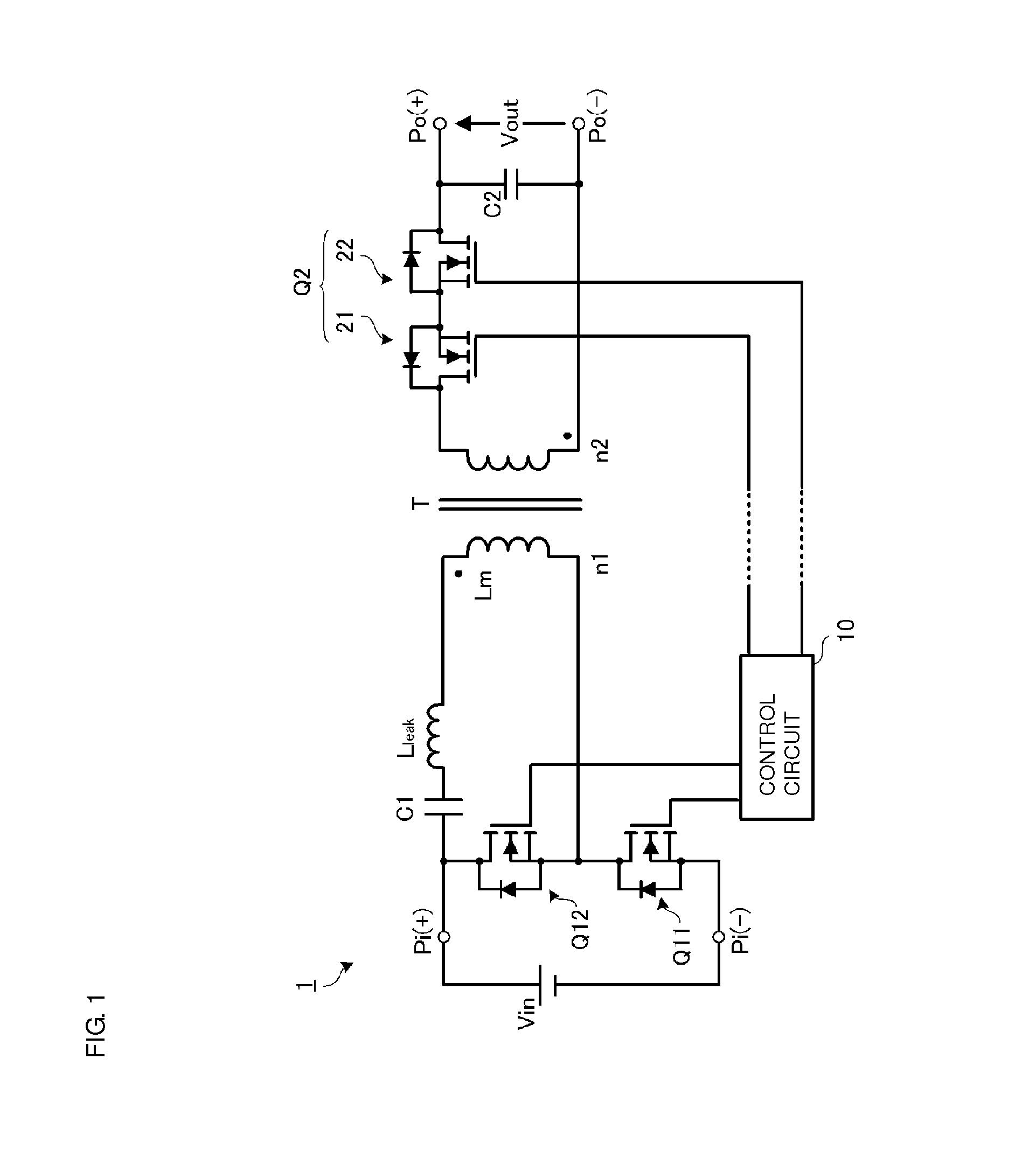
[0034]Hereafter, a switching power supply device equipped with an inverter device according to a preferred embodiment of the present invention will be described. FIG. 1 illustrates an equivalent circuit of a switching power supply device according to Preferred Embodiment 1 of the present invention. A switching power supply device 1 according to this preferred embodiment preferably includes a transformer T including one primary winding and an one secondary winding and converts an input direct current voltage into an alternating current voltage and outputs the alternating current voltage.
[0035]The switching power supply device 1 includes the transformer T in which a primary winding n1 and a secondary winding n2 are magnetically coupled with each other. In the diagram, Lleak denotes a leakage inductance of the primary side of the transformer T and Lm denotes an excitation inductance. In FIG. 1, an equivalent circuit is illustrated in which the leakage inductance L...
embodiment 2
Preferred Embodiment 2
[0064]Hereafter, Preferred Embodiment 2 of the present invention will be described. The circuit configuration of the switching power supply device according to this preferred embodiment is preferably the same as that of Preferred Embodiment 1 and therefore description thereof will be omitted. In this preferred embodiment, switching control of the switching elements Q11, Q12 and Q2 is different from in Preferred Embodiment 1. This difference will be described hereafter.
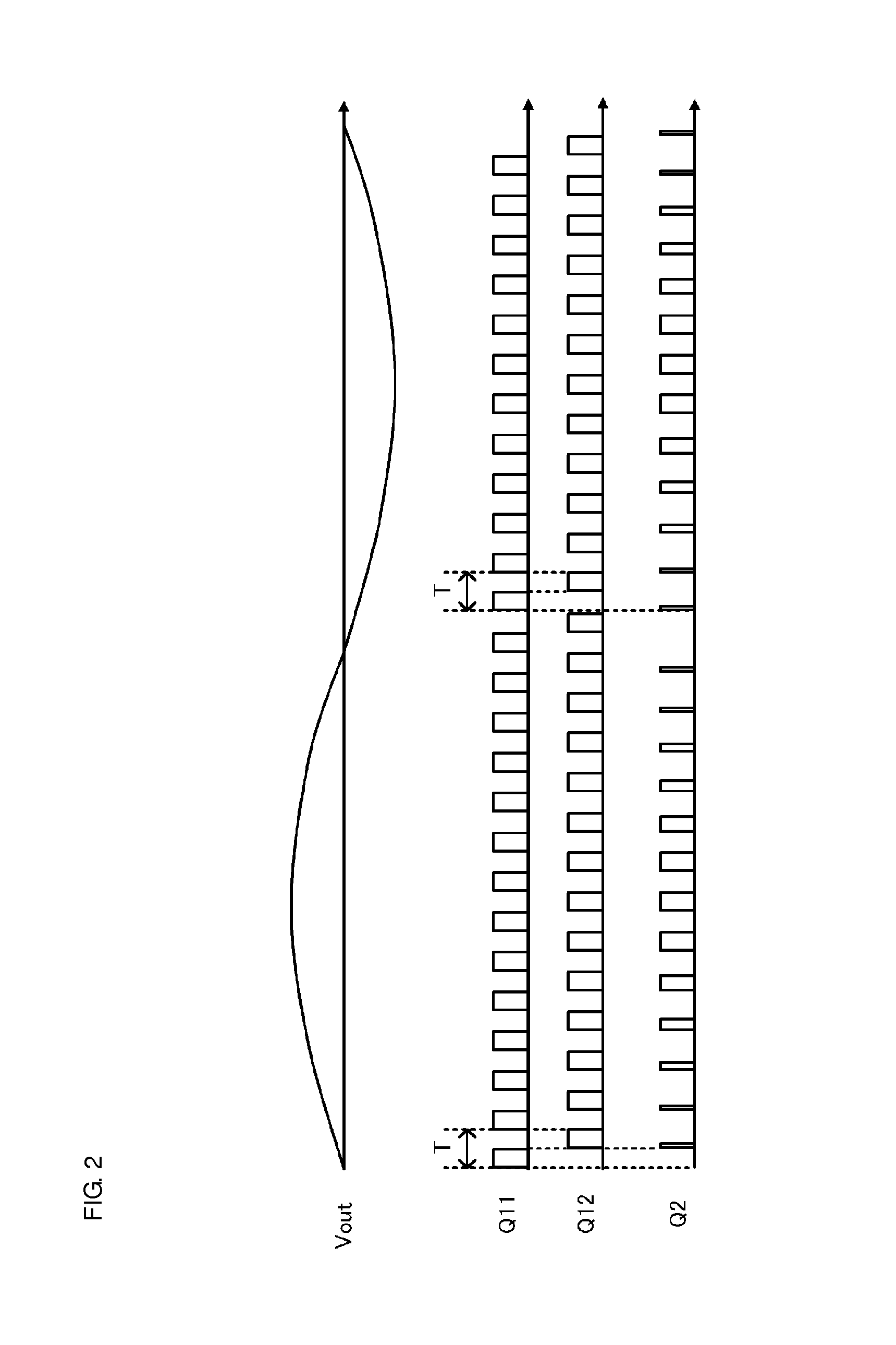
[0065]FIG. 5 illustrates the relationship between the on / off timing of the switching elements Q11, Q12 and Q2 and the alternating current voltage Vout output from the output terminals Po(+) and Po(−) in Preferred Embodiment 2. As a fundamental operation, similarly to as in Preferred Embodiment 1, the switching elements Q11 and Q12 are alternately switched on and off with a small dead time between their on periods. A positive voltage portion of the alternating current voltage is output by turning t...
embodiment 3
Preferred Embodiment 3
[0071]Hereafter, Preferred Embodiment 3 of the present invention will be described. The circuit configuration of the switching power supply device and the switching control of the switching elements Q11 and Q12 according to this preferred embodiment are preferably the same as in Preferred Embodiments 1 and 2 and therefore description thereof is omitted. In this preferred embodiment, switching control of the bidirectional switching element Q2 is different from in Preferred Embodiments 1 and 2. This difference will be described hereafter.
[0072]FIG. 7 illustrates the relationship between the on / off timing of the switching elements Q11, Q12 and Q2 and the alternating current voltage Vout output from the output terminals Po(+) and Po(−) in Preferred Embodiment 3. FIG. 8 illustrates current waveforms of the switching elements Q11 and Q12 and of the FET 21 of the bidirectional switching element Q2 at the time of output of a positive voltage portion of an alternating c...
PUM
 Abstract
Description
Claims
Application Information


