

Method for forming fin-shaped structure
- Summary
- Abstract
- Description
- Claims
- Application Information
AI Technical Summary
Benefits of technology
Problems solved by technology
Method used
Image

Examples
first embodiment
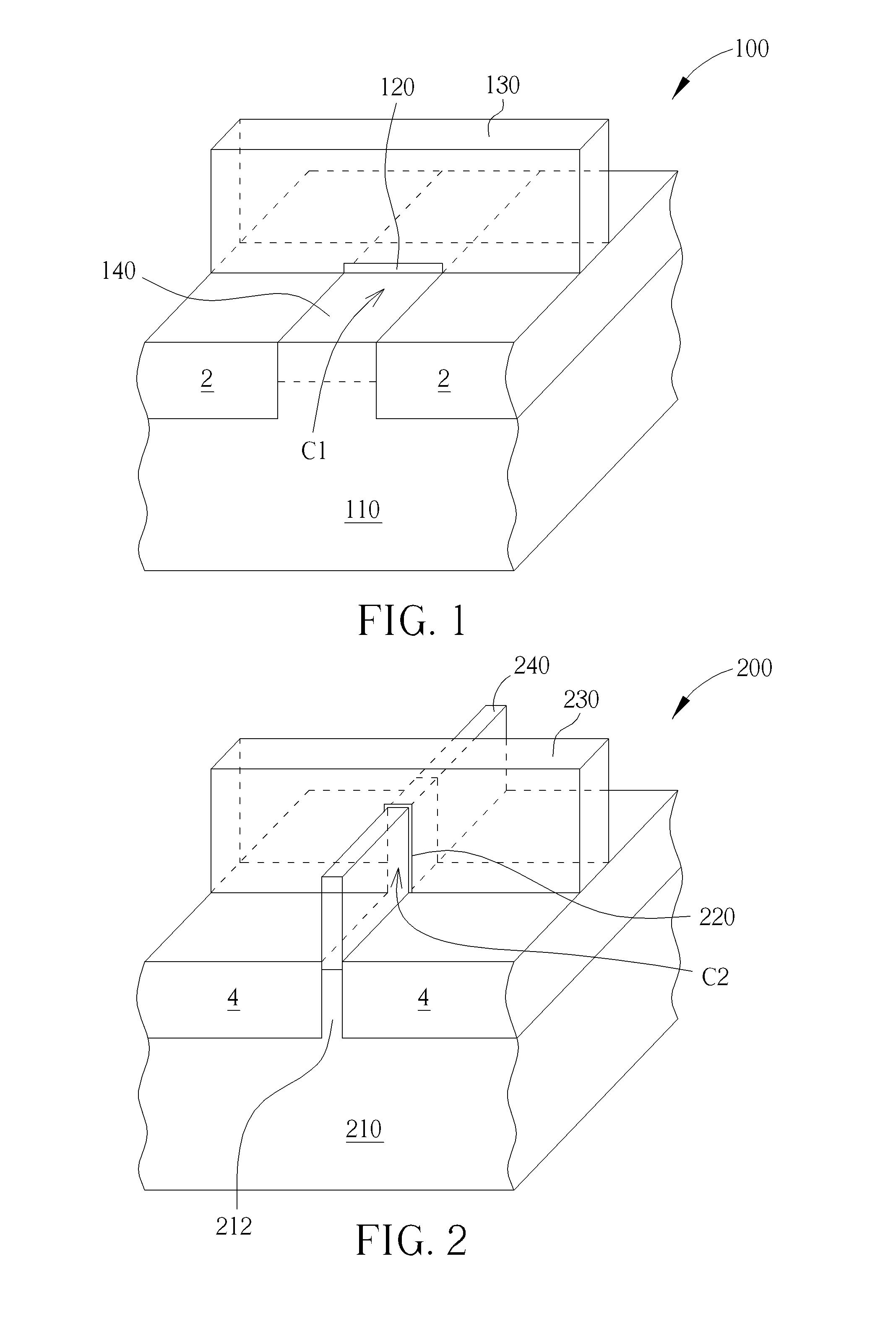
[0015]FIG. 1 schematically depicts a three-dimensional diagram of a planar transistor according to the present invention. As shown in FIG. 1, a planar transistor 100 includes a substrate 110, at least an isolation structure 2, a gate dielectric layer 120, an electrode 130 and a source / drain region 140. The substrate 110 may be a semiconductor substrate such as a silicon substrate, a silicon containing substrate such as a silicon carbide substrate, a III-V group-on-silicon (such as GaN-on-silicon) substrate, a graphene-on-silicon substrate, a silicon-on-insulator (SOI) substrate or an epitaxial layer containing a substrate such as a P-type substrate with a 2.5 μm P-type epitaxial layer. The isolation structure 2 is located in the substrate 110, wherein the isolation structure 2 is used to isolate each transistor formed on the substrate 110. The isolation structure 2 may be a shallow trench isolation (STI) structure, which may be formed through a shallow trench isolation (STI) process...
second embodiment
[0020]FIG. 2 schematically depicts a three-dimensional diagram of a multi-gate MOSFET according to the present invention. In FIG. 2 one example of a multi-gate MOSFET—a tri-gate MOSFET—is shown. A tri-gate MOSFET 200 may include a substrate 210, a fin-shaped structure 212, at least an isolation structure 4, a gate dielectric layer 220, an electrode 230 and a source / drain region 240.
[0021]The fin-shaped structure 212 is located on the substrate 210. Generally, the fin-shaped structure 212 and the substrate 210 form one piece only, but the fin-shaped structure 212 may be additionally formed on the substrate 210, depending upon the needs. The substrate 210 may be a semiconductor substrate such as a silicon substrate, a silicon containing substrate such as a silicon carbide substrate, a III-V group-on-silicon (such as GaN-on-silicon) substrate, a graphene-on-silicon substrate, a silicon-on-insulator (SOI) substrate or an epitaxial layer containing substrate such as a P-type substrate wi...
third embodiment
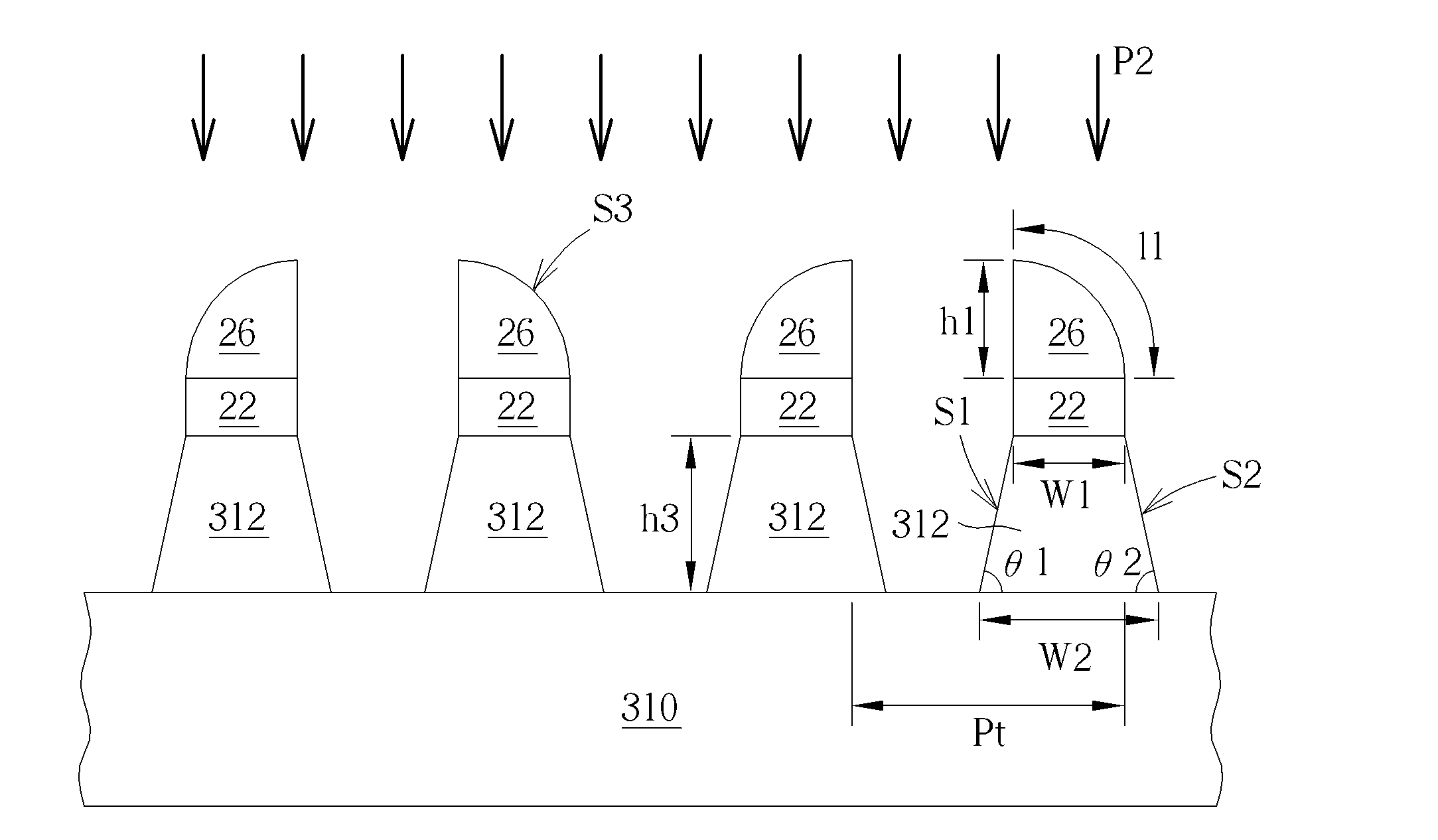
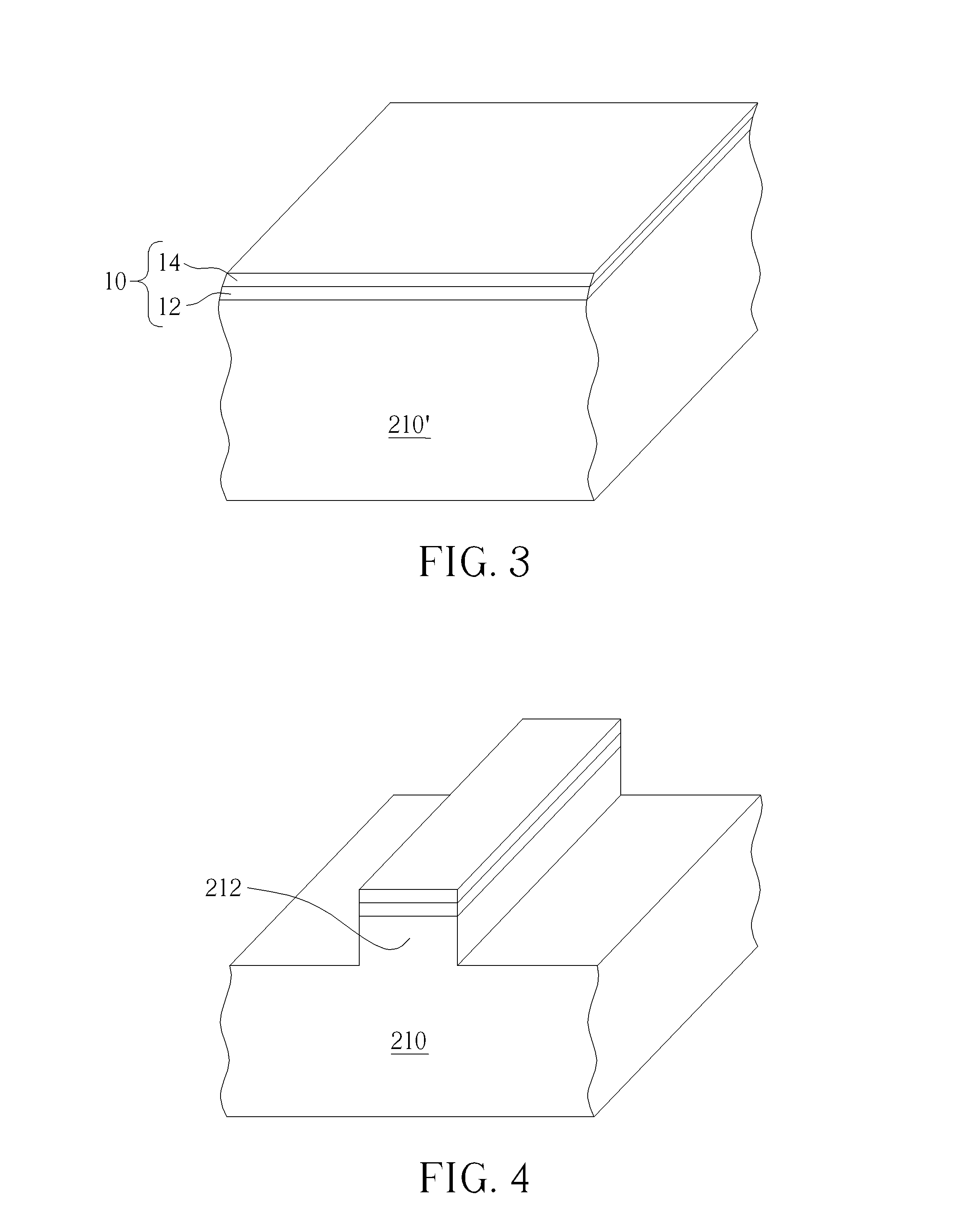
[0032]FIGS. 5-10 schematically depict cross-sectional views of a method for forming a fin-shaped structure according to the present invention. As shown in FIG. 5, a substrate 310 is provided, wherein the substrate 310 may be a semiconductor substrate such as a silicon substrate, a silicon containing substrate such as a silicon carbide substrate, a III-V group-on-silicon (such as GaN-on-silicon) substrate, a graphene-on-silicon substrate, a silicon-on-insulator (SOI) substrate or an epitaxial layer containing substrate such as a P-type substrate with a 2.5 μm P-type epitaxial layer. A pad layer 22 is formed on the substrate 310, wherein the pad layer 22 may include an oxide layer, but it is not limited thereto. A sacrificial pattern material 24′ is formed to entirely cover the pad layer 22. As shown in FIG. 6, the sacrificial pattern material 24′ is patterned to form a sacrificial pattern 24. In this embodiment, the sacrificial pattern material 24′ is polysilicon, and the sacrificial...
PUM
 Abstract
Description
Claims
Application Information