Liquid crystal display device and method of fabricating the same

a technology of liquid crystal display and adhesive layer, which is applied in the direction of instruments, optical light guides, optics, etc., can solve the problems of large contact area, complicated fabrication process for rework, and limited thickness of adhesive layer, so as to prevent light leakage or non-uniform luminance deterioration

Active Publication Date: 2014-08-28
LG DISPLAY CO LTD
View PDF3 Cites 34 Cited by
  • Summary
  • Abstract
  • Description
  • Claims
  • Application Information

AI Technical Summary

Benefits of technology

[0025]Another object of the present disclosure is to provide a liquid crystal display device where deterioration such as a

Problems solved by technology

However, the larger contact area is limited due to design rule and the thicker adhesive layer is limited due to a thin light shielding tape 61.
Since the abnormal disposition of the LED assembly 29

Method used


Image

  • Liquid crystal display device and method of fabricating the same
  • Liquid crystal display device and method of fabricating the same
  • Liquid crystal display device and method of fabricating the same

Examples


first embodiment

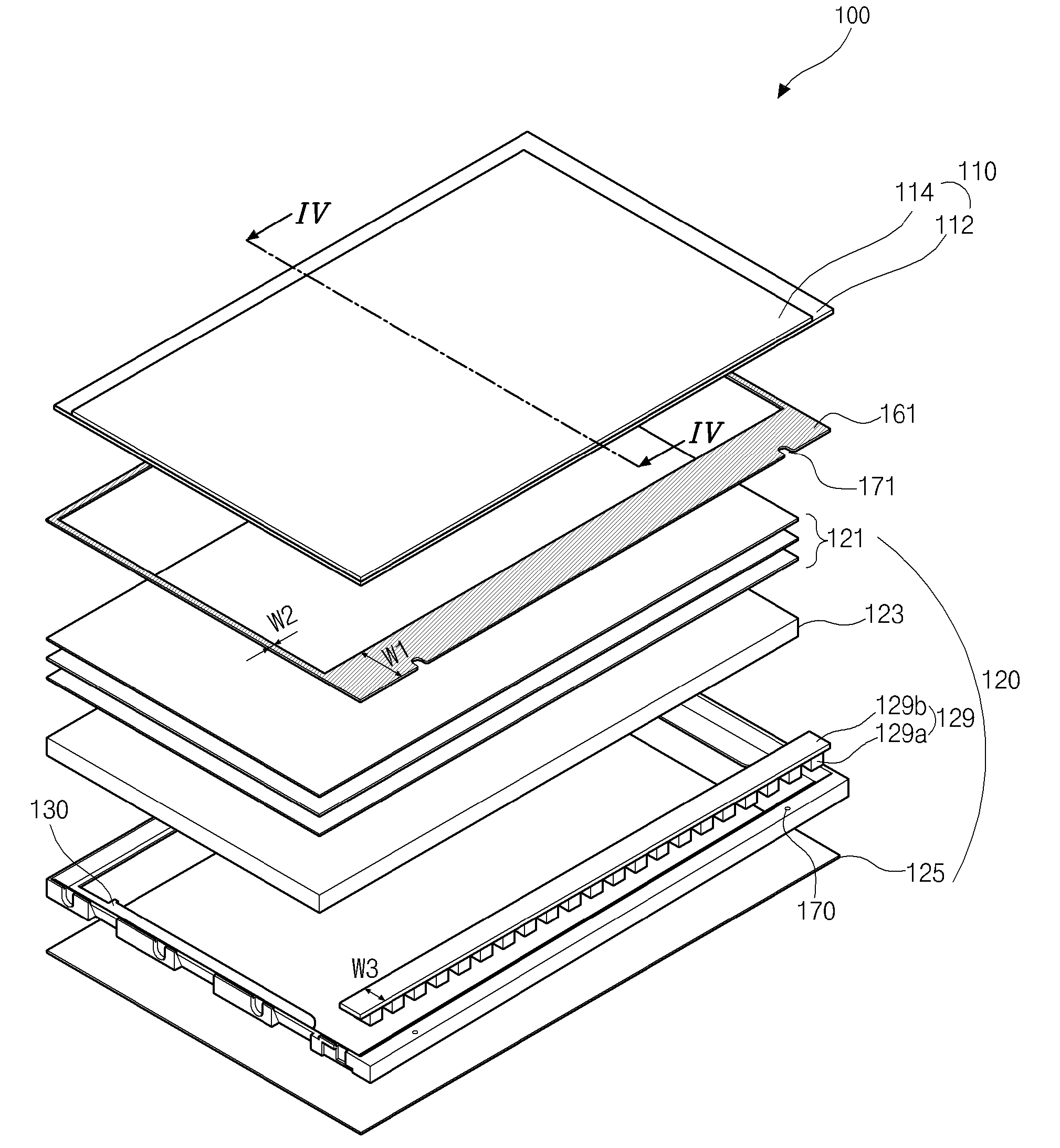
[0041]FIG. 3 is an exploded perspective view showing a liquid crystal display device according to the present invention, and FIG. 4 is a cross-sectional view taken along a line IV-IV of FIG. 3. Although a liquid crystal display device 100 is modularized by a main frame 130 without a bottom frame and a top frame for a thin profile in FIGS. 3 and 4, a liquid crystal display device may be modularized by a bottom frame, a main frame and a top frame in another embodiment.

[0042]In FIG. 3, a liquid crystal display (LCD) device 100 includes a liquid crystal panel 110, a backlight unit 120, a main frame 130 and a light shielding tape 161. The liquid crystal panel 110 for displaying an image includes first and second substrates 112 and 114 and a liquid crystal layer (not shown) between the first and second substrates 112 and 114.

[0043]Although not shown, when the LCD device 100 has an active matrix type, a gate line and a data line are formed on an inner surface of the first substrate 112, wh...

second embodiment

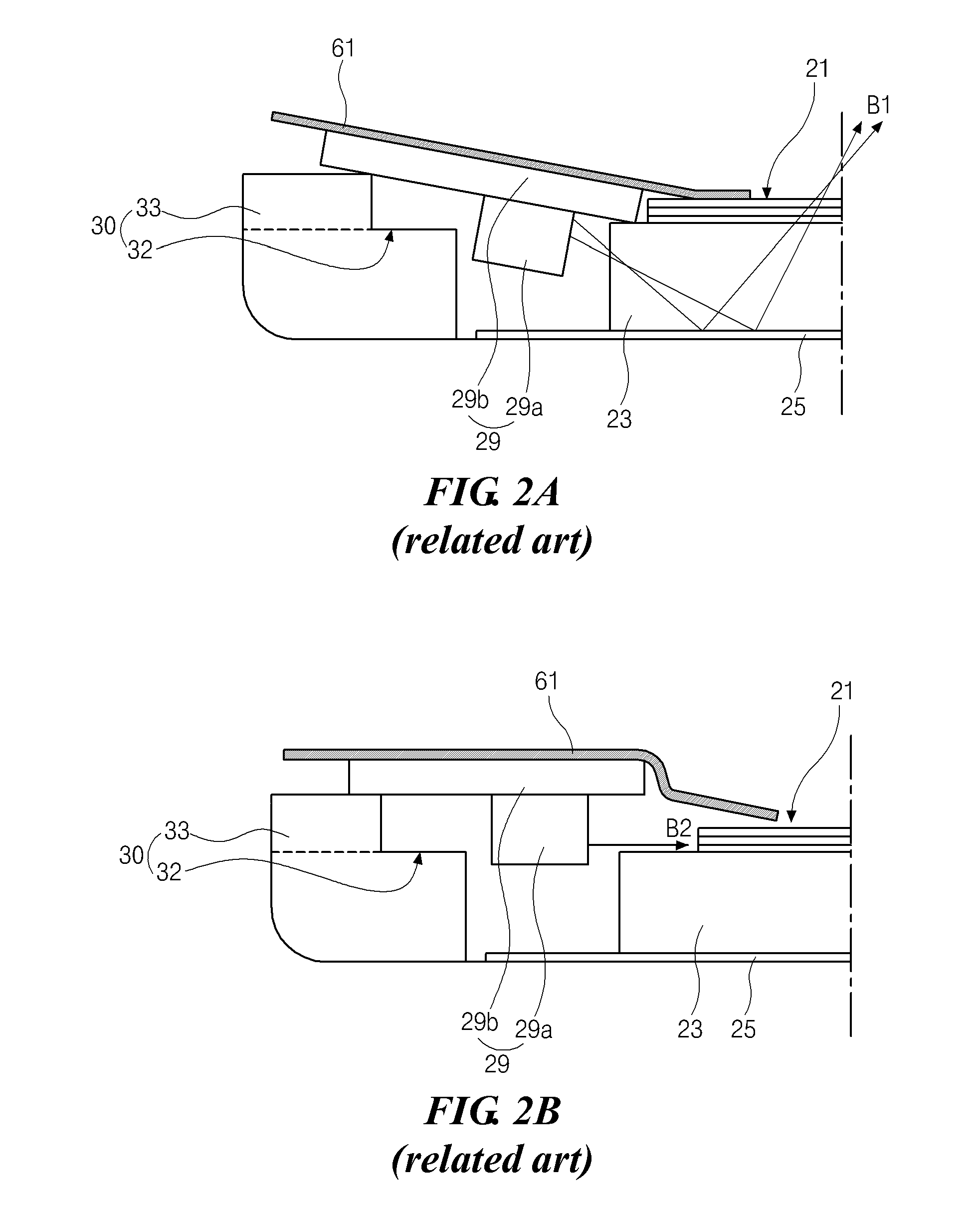
[0077]FIG. 9 is a cross-sectional view showing an edge portion of a liquid crystal display device according to the present invention.

[0078]In FIG. 9, an LED assembly 229 including a plurality of LEDs 229a and an FPCB 229b is disposed on a main frame 230 including a flat portion 232 and a guide wall 233. For example, the FPCB 229b may be disposed on the flat portion 232, and an edge portion of the FPCB 229b may be aligned to an edge portion of the guide wall 233. The guide wall 233 has at least one concave portion 270.

[0079]In addition, a light shielding tape 261 having at least one open portion 271 is formed on the main frame 230 and the LED assembly 229. For example, the light shielding tape 261 may be attached to the guide wall 233 and the FPCB 229b, and the at least one open portion 271 may expose the at least one concave portion 270.

[0080]The at least one concave portion 270 may have a groove shape such that the at least one concave portion 270 is formed in an upper portion of t...


PUM

PropertyMeasurementUnit
Shapeaaaaaaaaaa
Widthaaaaaaaaaa

Abstract

A liquid crystal display device includes: a liquid crystal panel; a backlight unit under the liquid crystal panel, the backlight unit including a light emitting diode (LED) assembly supplying a light and a light guide plate transmitting the light from the LED assembly to the liquid crystal panel; a main frame surrounding the backlight unit, the main frame including a flat portion for supporting the LED assembly and a guide wall for guiding the LED assembly, the guide wall including at least one concave portion; and a light shielding tape on the guide wall and the LED assembly, the light shielding tape including at least one open portion corresponding to the at least one concave portion.

Description

CROSS REFERENCE TO RELATED APPLICATIONS[0001]The present application claims the benefit of priority of Korean Patent Application No. 10-2013-0021171 filed in the Republic of Korea on Feb. 27, 2013, which is hereby incorporated by reference in its entirety.BACKGROUND OF THE INVENTION[0002]1. Field of the Disclosure[0003]The present disclosure relates to a liquid crystal display device. The present disclosure also relates to a liquid crystal display device where deterioration such as a light leakage or a non-uniformity in luminance is prevented due to an open portion of a light shielding tape and a concave portion of a main frame and a method of fabricating the liquid crystal display device.[0004]2. Discussion of the Related Art[0005]As the information age progresses, display devices processing and displaying a large amount of information have been rapidly developed. Specifically, various flat panel displays (FPDs) such as a liquid crystal display (LCD) device, a plasma display panel ...

Claims


Application Information

Patent Timeline
IPC IPC(8): F21V8/00
CPCG02B6/0023G02B6/009G02B6/0088Y10T29/49002G02F1/133308G02F1/133608G02F1/133615G02F1/1345G02F1/1333
Inventor JUNG, YEOUN-JEI
Owner LG DISPLAY CO LTD
Why Eureka
Try Eureka