Semiconductor structure, method for forming the same and method for suppressing hot cluster

US20140246713A1Active Publication Date: 2014-09-04HIMAX IMAGING LIMITED

Image

  • Semiconductor structure, method for forming the same and method for suppressing hot cluster
  • Semiconductor structure, method for forming the same and method for suppressing hot cluster
  • Semiconductor structure, method for forming the same and method for suppressing hot cluster

Examples


Embodiment Construction

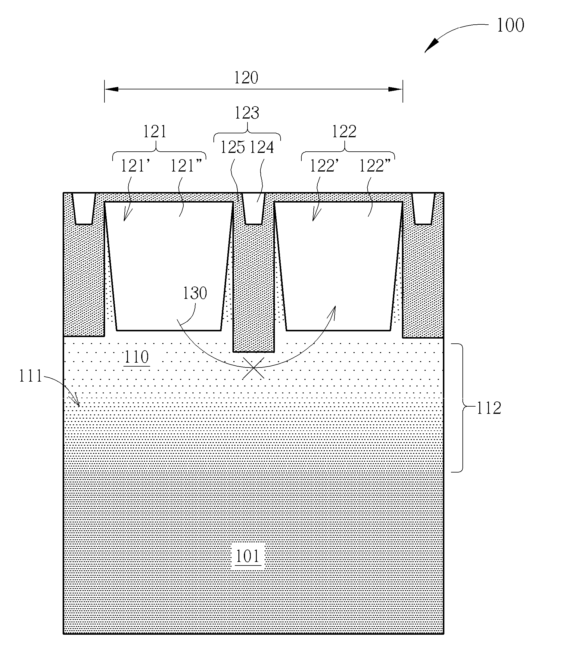
[0032]The present invention provides a method for forming a semiconductor structure to suppress a hot cluster and a resultant semiconductor structure for suppressing a hot cluster. Accordingly, the present invention further provides a method for suppressing a hot cluster. The method of the present invention may make the bad behaviors of an abnormal pixel locally restricted without spreading out to form a hot cluster. In such a way, the problem of the tendency of abnormal pixels to form a hot cluster may be effectively solved and the disaster of total failure of a die may be avoided because of a single hot cluster within.

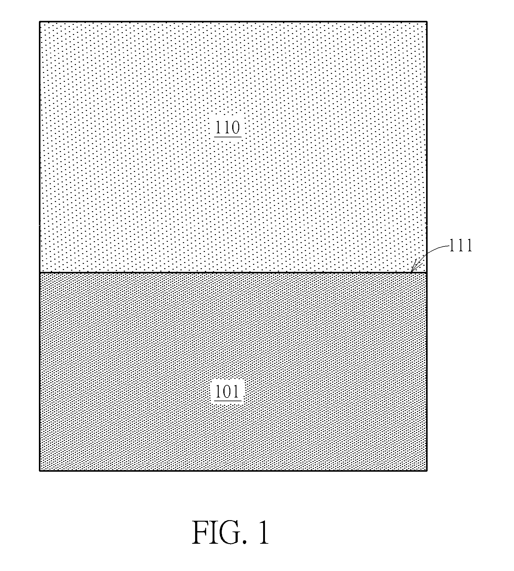
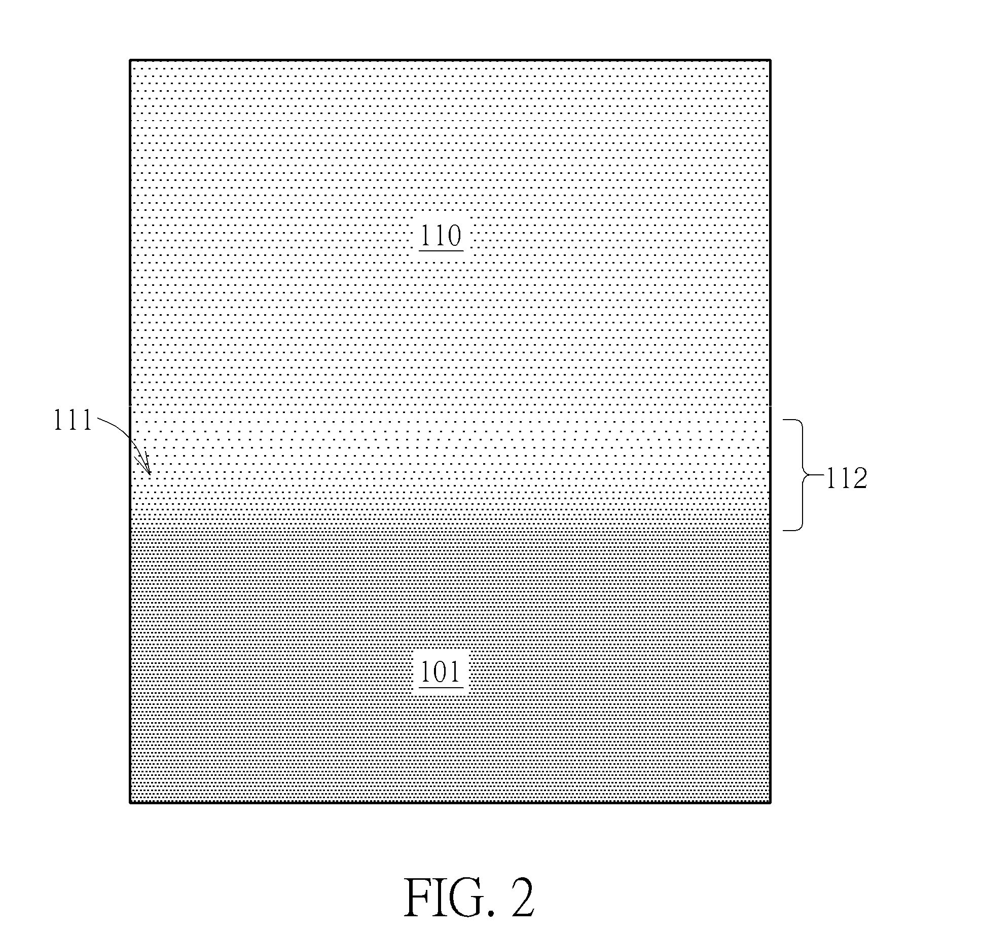
[0033]In a first aspect, the present invention provides a method for forming a semiconductor structure to suppress a hot cluster. In such a way, it is a possible to suppress a hot cluster. FIG. 1 to FIG. 4 illustrates the steps for forming a semiconductor structure to suppress a hot cluster. First, please refer to FIG. 1, a substrate 101 is provided and an epitaxial ...


PUM


Abstract

A semiconductor structure for suppressing hot clusters includes a substrate of a first dopant concentration, an epitaxial layer having a second dopant concentration smaller than the first dopant concentration and directly disposed on the substrate, a dopant gradient region disposed in the epitaxial layer and having a gradient decreasing from the substrate to the epitaxial layer, a shallow trench isolation disposed between a first element region and a second element region, and a shallow trench doping region surrounding the shallow trench isolation and near the dopant gradient region to suppress a hot cluster formed by the first element region to jeopardize the second element region.

Description

CROSS REFERENCE TO RELATED APPLICATION[0001]This application claims the benefit of Taiwanese Application 102107511, filed Mar. 4, 2013.BACKGROUND OF THE INVENTION[0002]1. Field of the Invention[0003]The present invention generally relates to a method for forming a semiconductor structure to suppress a hot cluster, a method for suppressing a hot cluster and a semiconductor structure for suppressing a hot cluster. In particular, the present invention is directed to a semiconductor structure with a dopant gradient region of a constructed back diffusion type as well as an isolation doping region surrounding a shallow trench isolation so that in the resultant semiconductor structure a shallow trench isolation region is substantially adjacent to the dopant gradient region to suppress a possible hot cluster in the semiconductor structure.[0004]2. Description of the Prior Art[0005]A CMOS image sensor is widely used in many applications, such as a portable device, a web cam, a monitor, a toy...

Claims


Application Information

Patent Timeline
04 Sep 2014
Publication
US20140246713A1
IPC
H01L27/146
CPC
H01L27/14687; H01L27/14689; H01L27/14643; H01L27/1463; H01L27/14645
Inventors
WU, YANG; YU, FEIXIA