Wafer-level test structure and test method for a DRAM chip

A test structure, wafer-level technology, applied in static memory, instruments, etc., can solve the problem of occupying chip area and increase cost, and achieve the effect of reducing chip area, improving utilization rate, and reducing chip area

Active Publication Date: 2017-12-26
XI AN UNIIC SEMICON CO LTD
View PDF4 Cites 0 Cited by
  • Summary
  • Abstract
  • Description
  • Claims
  • Application Information

AI Technical Summary

Problems solved by technology

Not only do you need to test a dedicated pin card during the test, which increases the cost, but also the test pads that will not be used during use will occupy the chip area and increase the cost.

Method used


Image

  • Wafer-level test structure and test method for a DRAM chip
  • Wafer-level test structure and test method for a DRAM chip
  • Wafer-level test structure and test method for a DRAM chip

Examples


Embodiment Construction

[0023] The present invention will be further described in detail below in conjunction with specific embodiments, which are explanations of the present invention rather than limitations.

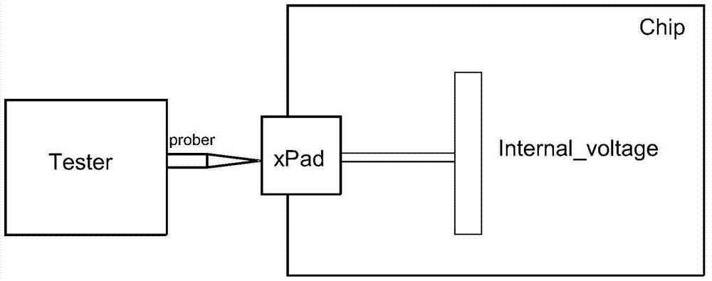
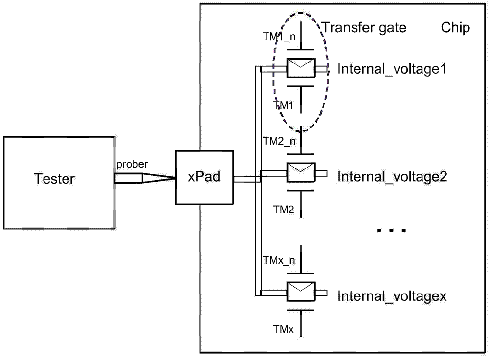
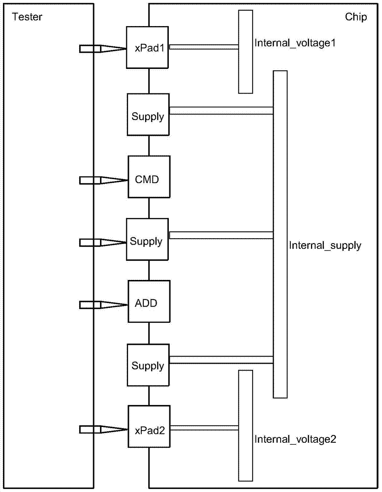
[0024] A wafer-level test structure of a DRAM chip of the present invention, such as Figure 4 As shown, it includes a first power supply pad and a second power supply pad respectively connected to the internal power supply network of the DRAM chip; the second power supply pad is connected to the internal power supply network through a power supply path, and the second power supply pad is connected to the internal voltage The network is set through the connection of the voltage path, and the voltage path is set in parallel on the power path; the voltage path and the power path are respectively connected to the first transmission gate and the second transmission gate through the input and output terminals, and the control of the first transmission gate and the second transmission gate The pola...


PUM


Abstract

A wafer-level test structure of a DRAM chip according to the present invention comprises a first power supply pad and a second power supply pad respectively connected to the internal power supply network of the DRAM chip; the second power supply pads are respectively connected to the internal power supply network through a power supply path The setting is to communicate with the internal voltage network through the voltage path, and the voltage path is set on the power path in parallel; the voltage path and the power path are respectively connected with the first transmission gate and the second transmission gate through the input and output terminals, and the first transmission gate and the second transmission gate are connected to each other. The control terminals of the two transmission gates have opposite polarities and are connected to the same control signal. The test method of the present invention is to connect the internal voltage network to the non-test power supply pad, and then respectively set transmission gates on the connection paths between the non-test power supply pad and the internal power supply network and the internal voltage network, two The control terminals of the transmission gate have opposite polarities and are connected to the same control signal; this power supply pad is used as a test pad during wafer-level testing.

Description

technical field [0001] The invention relates to a test of a DRAM chip, in particular to a wafer-level test structure and a test method of a DRAM chip. Background technique [0002] DRAM (Dynamic Random Access Memory, Dynamic Random Access Memory) is the most common system memory. There are various internal voltages in the DRAM chip. During the DRAM wafer level test (CP), the voltage network inside the chip needs to be measured and the voltage value should be adjusted accurately. Therefore, it is necessary to reserve additionally for the internal voltage test when designing the chip. Test pad (xPad) for probe contact to complete the test. These test pads are not standard package ports and will not be connected during back-end packaging, so they are invisible and useless to end customers. When testing the pad design, considering that it is invisible to end customers, it is always hoped that it should be as small as possible in order to reduce the consumption of chip area and...

Claims


Application Information

Patent Timeline
Patent Type & Authority Patents(China)
IPC IPC(8): G11C29/08G11C29/56
Inventor 王正文
Owner XI AN UNIIC SEMICON CO LTD
Why Eureka
Try Eureka