Semiconductor structure, method for forming the same and method for suppressing hot cluster

a semiconductor structure and hot cluster technology, applied in the direction of solid-state devices, electric devices, basic electric elements, etc., can solve the problems of total failure of the die, the failure of the original pixel, and the combination of normal and abnormal parts

Active Publication Date: 2016-09-06
HIMAX IMAGING LIMITED
View PDF4 Cites 0 Cited by
  • Summary
  • Abstract
  • Description
  • Claims
  • Application Information

AI Technical Summary

Benefits of technology

[0008]In the light of these, the present invention proposes a semiconductor structure for suppressing a hot cluster, a method for forming a semiconductor structure and a method for suppressing a hot cluster. The method of the present invention may make the behavior of an abnormal pixel locally restricted without spreading out to form a hot cluster. This may effectively solve the problem of the tendency of abnormal pixels to form a hot cluster and avoid the disaster of total failure of a die because of a single hot cluster.
[0014]In another embodiment of the present invention, the shallow trench isolation region and the dopant gradient region together form a potential barrier to suppress a hot cluster caused by a dark current travelling from the first element region through the epitaxial layer to the second element region.
[0022]In another embodiment of the present invention, the shallow trench isolation region substantially overlaps the dopant gradient region to suppress a dark current travelling from the first element region through the epitaxial layer to the second element region.
[0027]In another embodiment of the present invention, the shallow trench isolation region substantially overlap the dopant gradient region to suppress a dark current travelling from the first element region through the epitaxial layer to the second element region.

Problems solved by technology

A hot cluster failure is like a contagious disease, not only the functions of the original pixel are destroyed but also the neighboring pixels are also suffering collateral damages so that normal ones and abnormal ones together become bad ones.
Since the current product standards are demandingly high, only one single hot cluster failure results in the total failure of the die, no matter how good the others are.
So far the proposed ways to solve the hot cluster failure problems are still limited to case-by-case approaches.
There is no universal and thorough solution available.

Method used


Image

  • Semiconductor structure, method for forming the same and method for suppressing hot cluster
  • Semiconductor structure, method for forming the same and method for suppressing hot cluster
  • Semiconductor structure, method for forming the same and method for suppressing hot cluster

Examples


Embodiment Construction

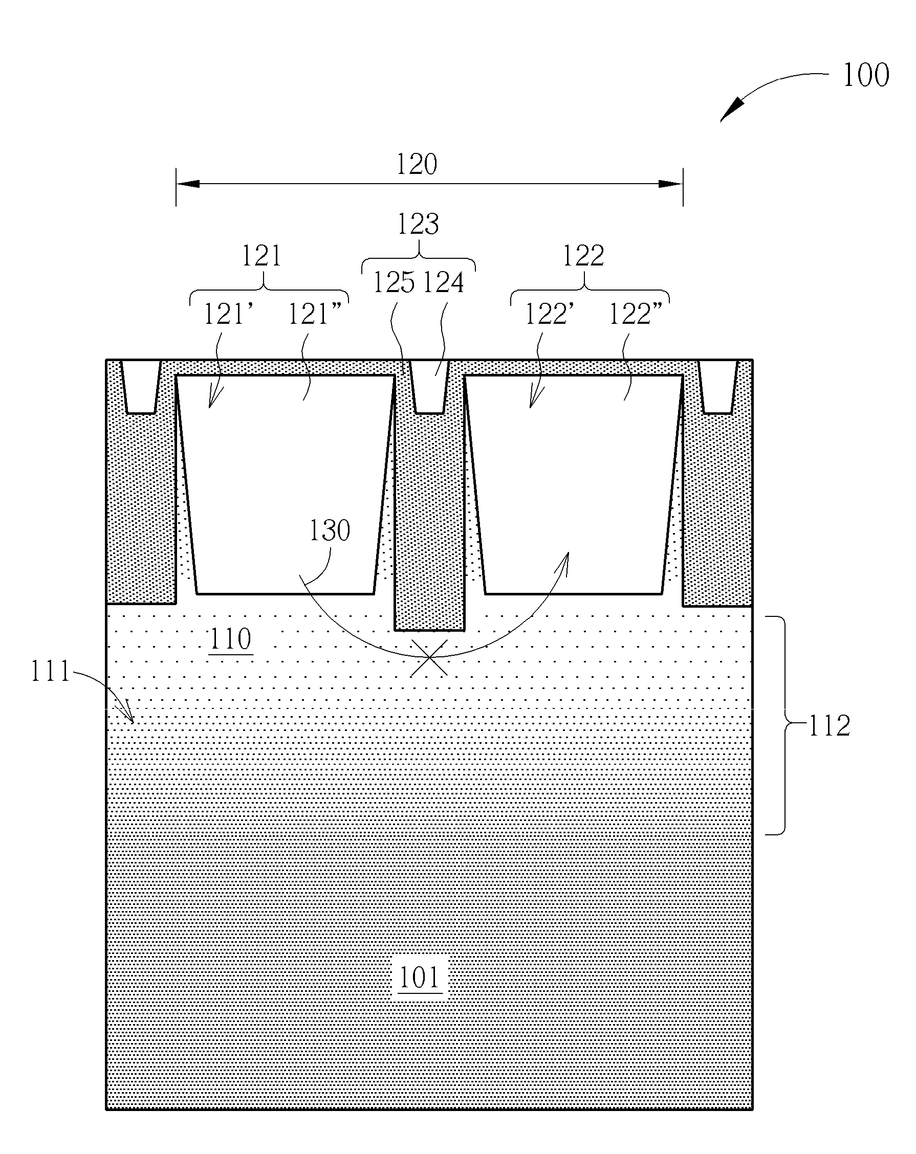
[0032]The present invention provides a method for forming a semiconductor structure to suppress a hot cluster and a resultant semiconductor structure for suppressing a hot cluster. Accordingly, the present invention further provides a method for suppressing a hot cluster. The method of the present invention may make the bad behaviors of an abnormal pixel locally restricted without spreading out to form a hot cluster. In such a way, the problem of the tendency of abnormal pixels to form a hot cluster may be effectively solved and the disaster of total failure of a die may be avoided because of a single hot cluster within.

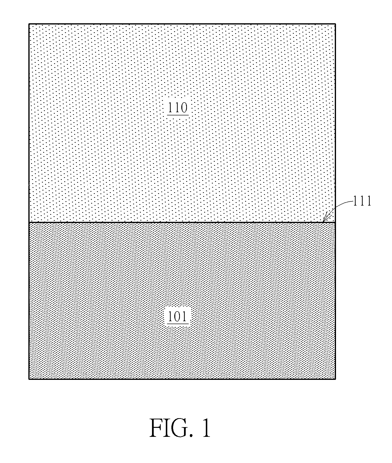
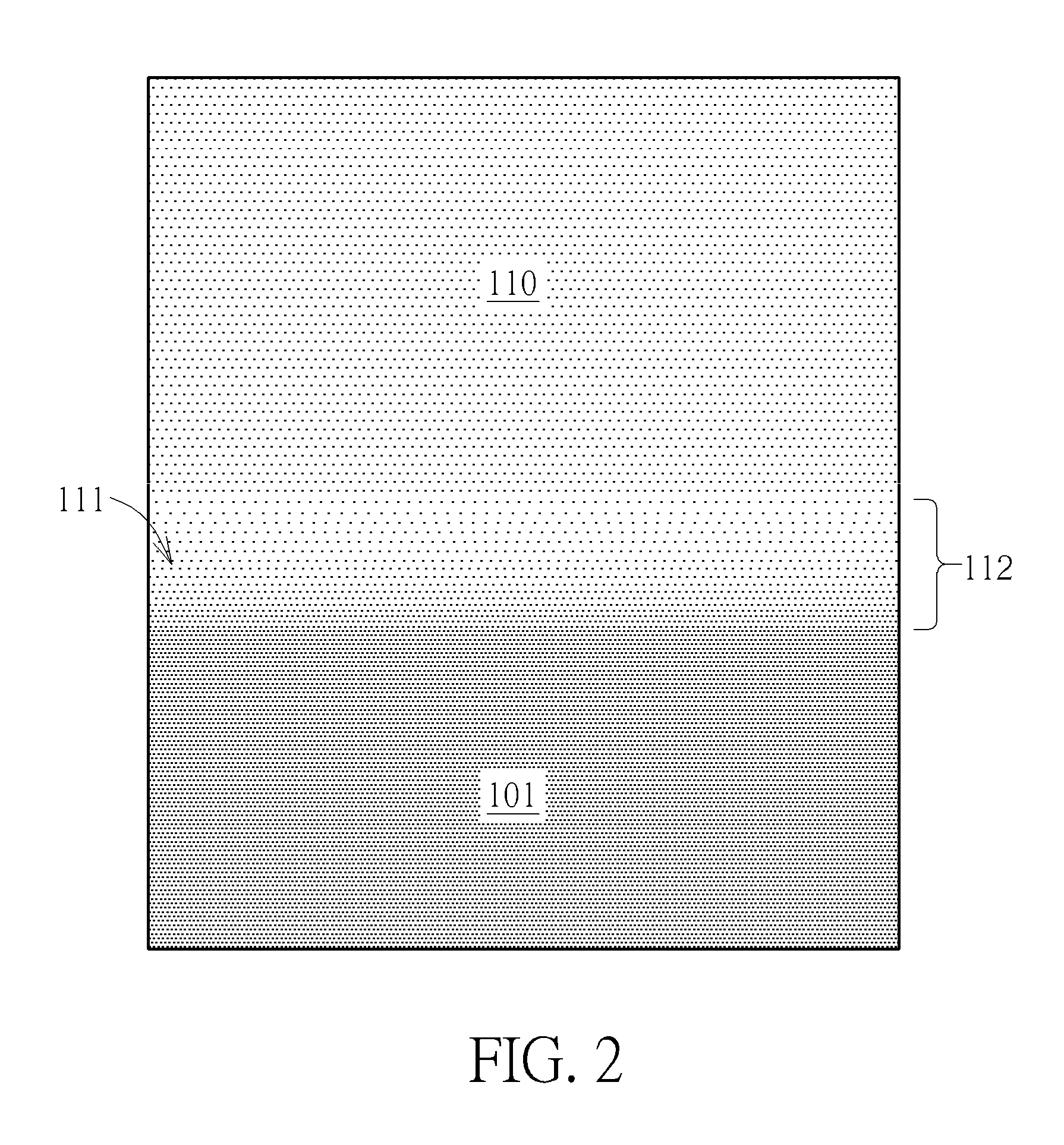
[0033]In a first aspect, the present invention provides a method for forming a semiconductor structure to suppress a hot cluster. In such a way, it is a possible to suppress a hot cluster. FIG. 1 to FIG. 4 illustrates the steps for forming a semiconductor structure to suppress a hot cluster. First, please refer to FIG. 1, a substrate 101 is provided and an epitaxial ...


PUM


Abstract

A semiconductor structure for suppressing hot clusters includes a substrate of a first dopant concentration, an epitaxial layer having a second dopant concentration smaller than the first dopant concentration and directly disposed on the substrate, a dopant gradient region disposed in the epitaxial layer and having a gradient decreasing from the substrate to the epitaxial layer, a shallow trench isolation disposed between a first element region and a second element region, and a shallow trench doping region surrounding the shallow trench isolation and near the dopant gradient region to suppress a hot cluster formed by the first element region to jeopardize the second element region.

Description

CROSS REFERENCE TO RELATED APPLICATION[0001]This application claims the benefit of Taiwanese Application 102107511, filed Mar. 4, 2013.BACKGROUND OF THE INVENTION[0002]1. Field of the Invention[0003]The present invention generally relates to a method for forming a semiconductor structure to suppress a hot cluster, a method for suppressing a hot cluster and a semiconductor structure for suppressing a hot cluster. In particular, the present invention is directed to a semiconductor structure with a dopant gradient region of a constructed back diffusion type as well as an isolation doping region surrounding a shallow trench isolation so that in the resultant semiconductor structure a shallow trench isolation region is substantially adjacent to the dopant gradient region to suppress a possible hot cluster in the semiconductor structure.[0004]2. Description of the Prior Art[0005]A CMOS image sensor is widely used in many applications, such as a portable device, a web cam, a monitor, a toy...

Claims


Application Information

Patent Timeline
Patent Type & Authority Patents(United States)
IPC IPC(8): H01L27/00H01L27/146
CPCH01L27/14687H01L27/1463H01L27/14645H01L27/14689
Inventor WU, YANGYU, FEIXIACHANG, CHUNG-WEI
Owner HIMAX IMAGING LIMITED
Why Eureka
Try Eureka