Substrate processing method

a processing method and substrate technology, applied in the direction of manufacturing tools, cleaning with liquids, lapping machines, etc., can solve the problems of poor adhesion between the copper interconnect and the dielectric film, short circuit between the interconnects or current leakage, etc., to suppress the electrostatic charge of the substrate, and eliminate the static electricity

Active Publication Date: 2014-09-04
EBARA CORP
View PDF15 Cites 11 Cited by
  • Summary
  • Abstract
  • Description
  • Claims
  • Application Information

AI Technical Summary

Benefits of technology

[0010]The present invention has been made in view of the above circumstances. It is therefore an object of the present invention to provide a substrate processing method which can suppress electrostatic charge of a substrate having a structure (e.g., a dielectric film, a metallic film, or a device including a dielectric film and a metallic film) formed on a surface thereof.
[0019]As described above, once the dielectric film is electrostatically charged, it is almost impossible to eliminate the static electricity from the dielectric film. In view of this fact, the embodiment of this method suppresses the electrostatic charge of the substrate, instead of eliminating the static electricity that has been charged. Specifically, the surface of the substrate is irradiated with the soft X-rays while the pure water is being supplied onto the substrate. The irradiation of the substrate with the soft X-rays is started at the same time as or before the supply of pure water onto the substrate is started, and the irradiation of the substrate with the soft X-rays is stopped after the supply of the pure water onto the substrate is stopped. In other words, the substrate is irradiated with the soft X-rays at all times when the pure water forms a flow on the substrate. Therefore, it is possible to suppress the electrostatic charge of the substrate while supplying the pure water onto the substrate to process (e.g., rinse) the substrate.

Problems solved by technology

The electrostatic charge of the substrate surface may cause reattachment of particles that have been once removed by the cleaning process of the substrate surface, and may cause destruction of devices due to electrostatic discharge.
Consequently, shortcut between the interconnects or leakage of current may occur, and / or poor adhesion between the copper interconnects and the dielectric film may occur.
Since the electrostatic charge of the substrate surface can lower a reliability of the devices, it is necessary to eliminate static electricity from the substrate.
However, once a dielectric film, such as a TEOS film, is electrostatically charged, it is extremely difficult to remove the static electricity from the dielectric film. FIG. 1 is a graph showing results of an experiment for removing the static electricity from a TEOS film and PVC (polyvinyl chloride).
This means that the static electricity cannot be removed from the TEOS film by the soft X-ray irradiation.

Method used


Image

  • Substrate processing method
  • Substrate processing method
  • Substrate processing method

Examples


Embodiment Construction

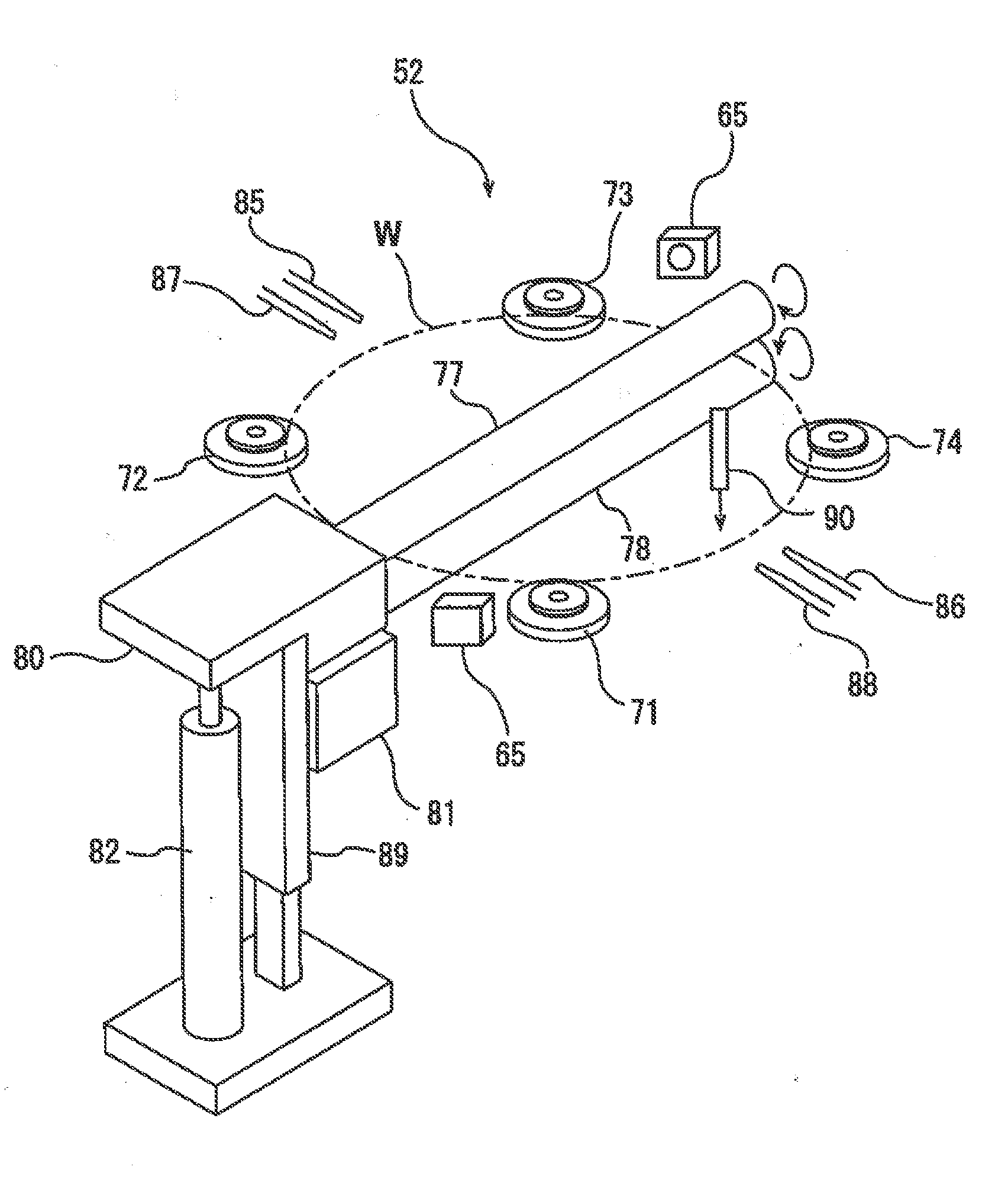
[0031]Embodiments will be described below with reference to the drawings. FIG. 3 is a view showing a polishing apparatus having a polishing omit, a cleaning unit, and a drying unit. This polishing apparatus is a substrate processing apparatus capable of performing a series of processes including polishing, cleaning, and drying of a wafer (or a substrate). As shown in FIG. 3, the polishing apparatus has a housing 2 in approximately a rectangular shape. An interior space of the housing 2 is divided by partitions 2a, 2b into a load-unload section 6, a polishing section 1, and a cleaning section 8. The polishing apparatus includes an operation controller 10 configured to control wafer processing operations.

[0032]The load-unload section 6 has load ports 12 on which wafer cassettes are placed, respectively. A plurality of wafers are stored in each wafer cassette. The load-unload section 6 has a moving mechanism 14 extending along an arrangement direction of the load ports 12. A transfer r...


PUM

PropertyMeasurementUnit
areaaaaaaaaaaa
dielectricaaaaaaaaaa
specific resistanceaaaaaaaaaa

Abstract

A substrate processing method includes rotating a substrate about a central axis thereof; starting irradiation of a surface of the substrate with soft X-rays; simultaneously with or after starting the irradiation of the surface of the substrate with the soft X-rays, starting supply of pure water onto the surface of the substrate; stopping the supply of the pure water onto the surface of the substrate; and then stopping the irradiation of the surface of the substrate with the soft X-rays.

Description

CROSS REFERENCE TO RELATED APPLICATIONS[0001]This document claims priorities to Japanese Patent Application No. 2013-41149 filed Mar. 1, 2013 and Japanese Patent Application No. 2014-24551 filed Feb. 12, 2014, the entire contents of which are hereby incorporated by reference.BACKGROUND OF THE MENTION[0002]1. Field of the Invention[0003]The present invention relates to a method of processing (e.g., rinsing) a substrate with pure water or ultrapure water, and especially relates to a substrate processing method of processing a substrate while suppressing electrostatic charge of a structure (e.g., a dielectric film, a metallic film, or a device including a dielectric film and a metallic film) formed on the substrate.[0004]2. Description of the Related Art[0005]In a manufacturing process of a semiconductor device, various films having different physical properties are formed on a silicon substrate and these films are subjected to various processes, thus forming fine metal interconnects. ...

Claims


Application Information

Patent Timeline
Patent Type & Authority Applications(United States)
IPC IPC(8): H01L21/306
CPCH01L21/306B24B37/10B24B37/34B24B49/12H01L21/02065H01L21/02074H01L21/67028H01L21/67034H01L21/67046H01L21/67051H01L21/67115B08B3/00B08B3/02B08B3/024B08B3/04B08B7/00B08B7/0035B08B7/005B08B7/0057H01L21/0206
Inventor ISHIBASHI, TOMOATSU
Owner EBARA CORP
Why Eureka
Try Eureka