Display device and electronic device

a technology of electronic devices and display devices, applied in the direction of static indicating devices, instruments, etc., can solve the problems of limited display regions and serious limitations in housing design, and achieve the effect of reducing frame width, high degree of flexibility of display regions, and less limitation of design flexibility

Inactive Publication Date: 2014-09-11
SEMICON ENERGY LAB CO LTD
View PDF8 Cites 105 Cited by
  • Summary
  • Abstract
  • Description
  • Claims
  • Application Information

AI Technical Summary

Benefits of technology

[0014]In view of the above problems, an object of one embodiment of the present invention is to provide a display device which can achieve a reduced frame width and of which the shape of the frame is the same as or similar to the shape of a display region even in the case where the display region has a non-rectangular shape. Another object of one embodiment of the present invention is to provide a display device which can achieve a reduced frame width and of which the shape of the frame is the same as or similar to the shape of a display region even in the case where the display region has high design flexibility. Another object of one embodiment of the present invention is to provide driver circuits of a display device which can achieve a reduced frame width and of which the shape of the frame is the same as or similar to the shape of a display region even in the case where the display region has high design flexibility. Another object of one embodiment of the present invention is to provide a display device having a novel structure.
[0017]According to one embodiment of the present invention, a high degree of flexibility of the shape of a display region and minimization of the outside shape of a display device with a reduced frame width can be achieved; thus, a display device with less limitation of design flexibility can be provided.

Problems solved by technology

In the case of such a method, limitation of housing design becomes serious even if the display region can have a non-rectangular shape.
However, in this method, at least one vertex of the display region is needed between a data driver (source driver) and a gate driver, and thus, the display region is limited.

Method used


Image

  • Display device and electronic device
  • Display device and electronic device
  • Display device and electronic device

Examples


embodiment 1

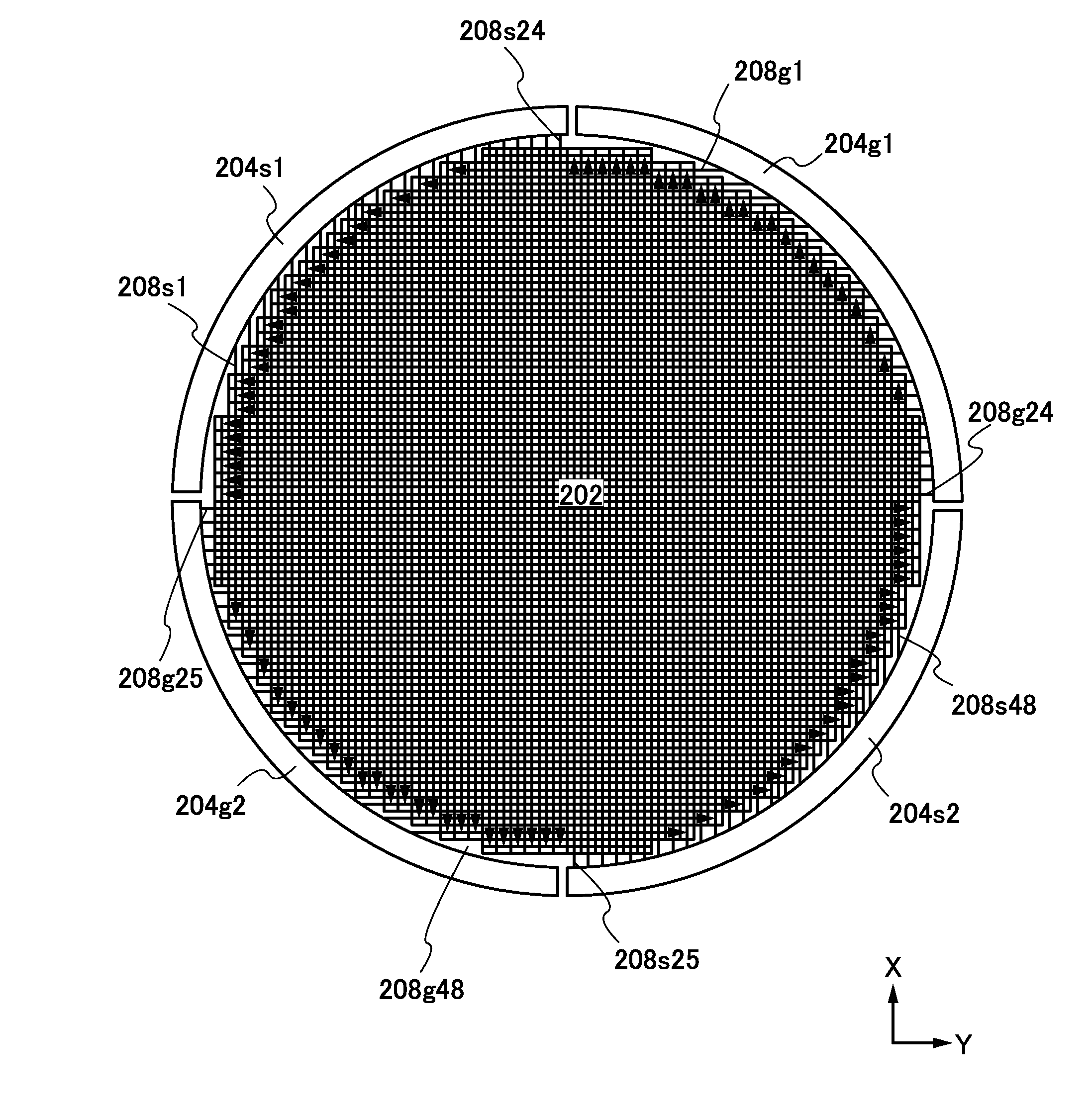
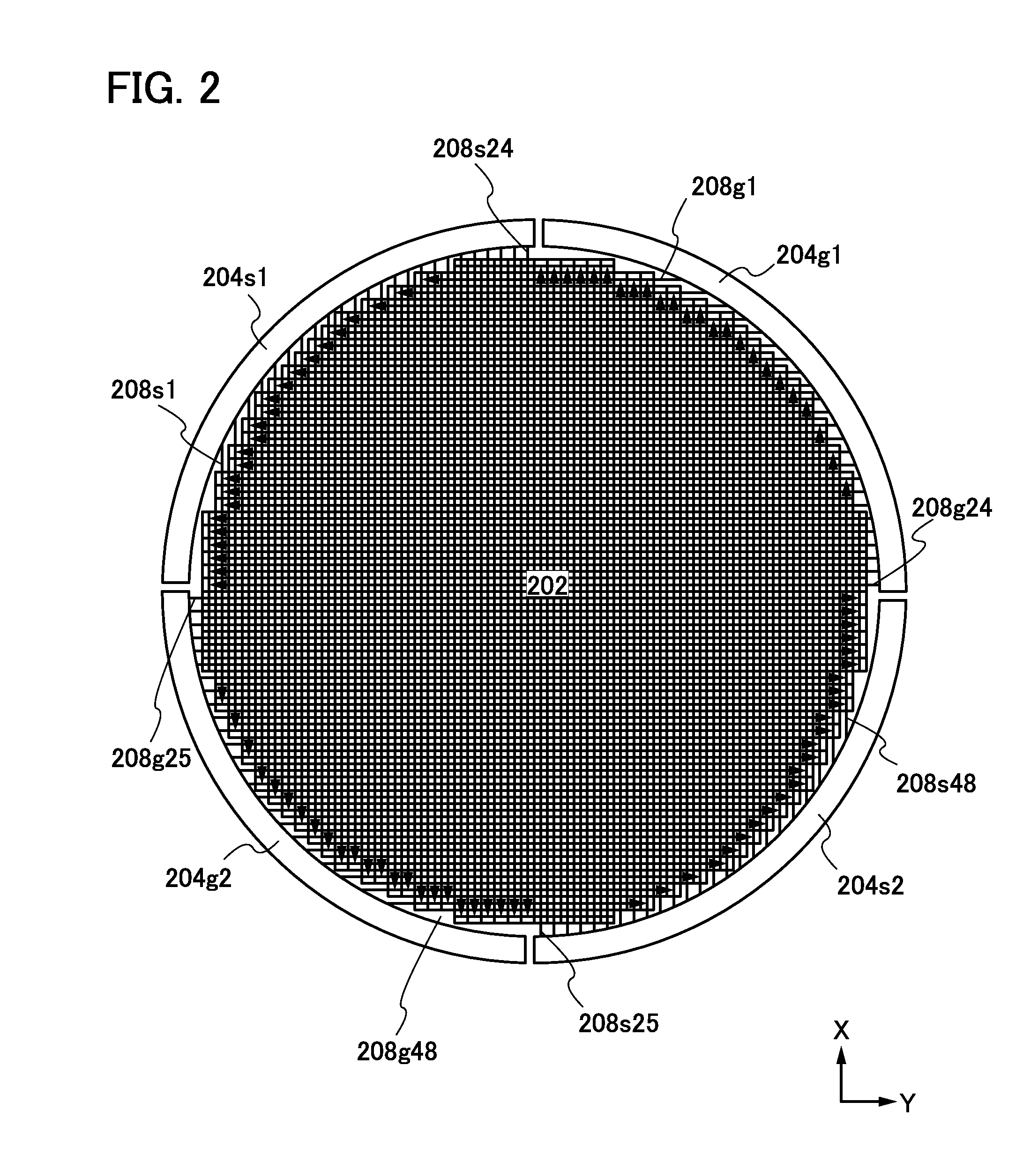
[0032]In this embodiment, a display device of one embodiment of the present invention will be described with reference to FIGS. 1A and 1B, FIG. 2, FIG. 3, and FIGS. 4A and 4B.

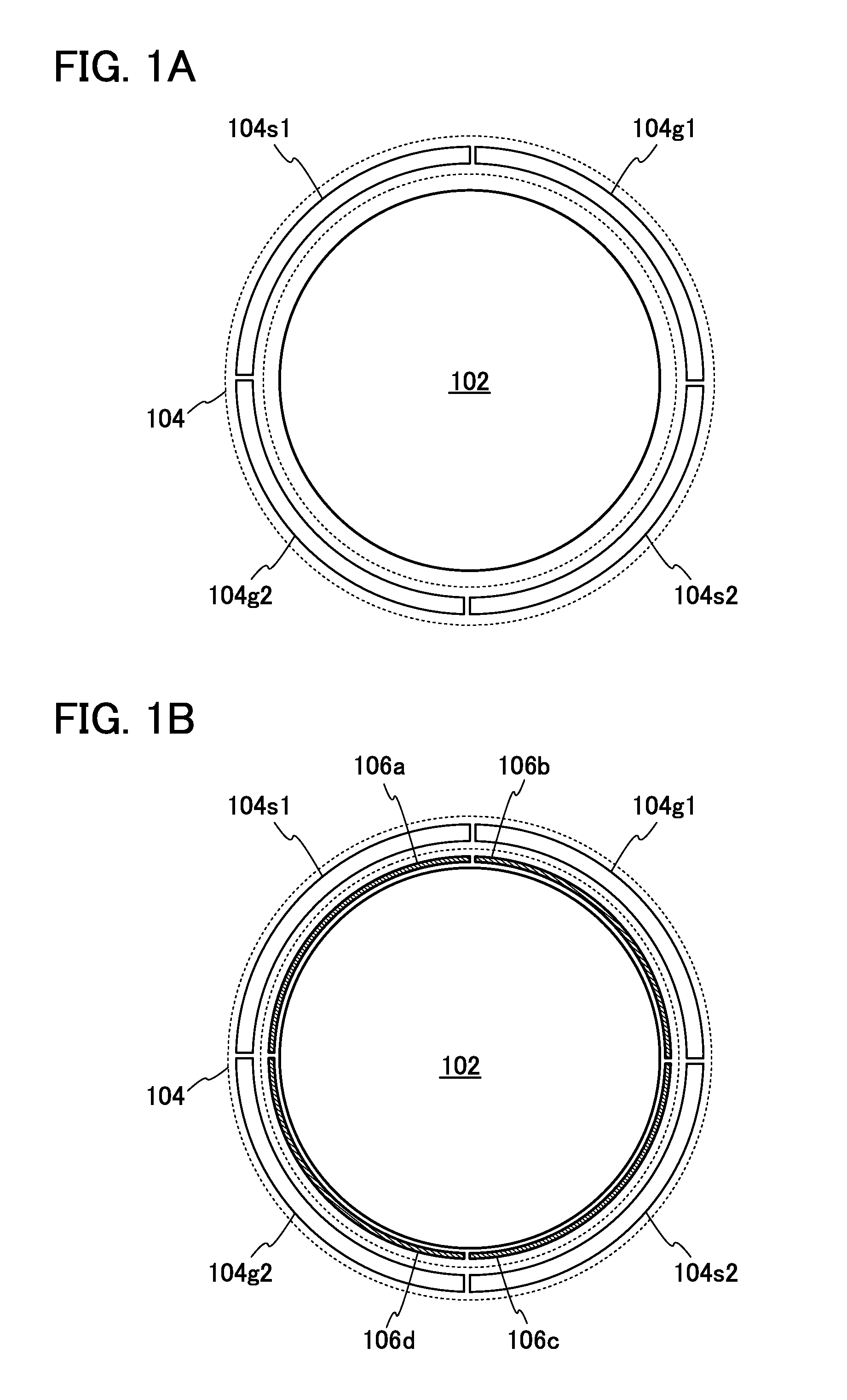
[0033]FIGS. 1A and 1B each illustrate an example of a display device of one embodiment of the present invention. Note that FIGS. 1A and 1B each illustrate the top view of the display device schematically.

[0034]The display devices in FIGS. 1A and 1B each include a circular display region. Note that the display region is not limited to a circular shape, and any shape may be used as long as it has a non-rectangular shape. As examples of a non-rectangular shape, a variety of shapes such as a polygonal shape having more than or equal to five corners, a regular circle shape, an oval shape, and a shape including an arc and a straight line can be given.

[0035]The display device in FIG. 1A includes a non-rectangular display region 102 and a driver circuit portion 104 on the periphery of the non-rectangular display region...

embodiment 2

[0072]In this embodiment, structures of display devices which are different from those described in Embodiment 1 will be described with reference to FIGS. 5A to 5C.

[0073]FIGS. 5A to 5C are schematic top views each illustrating a display device of one embodiment of the present invention.

[0074]Note that in FIGS. 5A to 5C, directions of arrows in the diagrams each indicate a direction in which a scan line or a signal line which is connected to a driver circuit is controlled.

[0075]The display device in FIG. 5A, which is a modification example of the display device in FIG. 1A, includes a non-rectangular display region 402 and a driver circuit portion on the periphery of the non-rectangular display region 402. The driver circuit portion includes a first gate driver 404g1, a second gate driver 404g2, a third gate driver 404g3, a fourth gate driver 404g4, a first source driver 404s1, a second source driver 404s2, a third source driver 404s3, and a fourth source driver 404s4.

[0076]Note that ...

embodiment 3

[0096]In this embodiment, a circuit configuration which can be used for a pixel circuit portion included in the display region 102 in FIG. 1A is described with reference to FIGS. 6A and 6B. Then, a circuit configuration which can be used for the protection circuits 106a, 106b, 106c, and 106d in FIG. 1B is described with reference to FIGS. 6C and 6D. Note that common reference numerals are used for portions having functions similar to those in the above embodiments, and detailed description of the portions is omitted.

[0097]First, circuit configurations in FIGS. 6A and 6B are described below.

[0098]A pixel circuit portion 510 in FIG. 6A includes a liquid crystal element 504, a transistor 502_1, and a capacitor 506_1.

[0099]As the transistor 502_1, a thin film transistor (TFT) formed over a glass substrate or a plastic substrate can be used, for example. Either a staggered TFT or an inverted staggered TFT may be employed. As a semiconductor material used for the TFT, amorphous silicon, p...


PUM


Abstract

To provide a display device which can achieve a reduced frame width and of which the shape of the frame is the same as or similar to the shape of a display region even in the case where the display region has a non-rectangular shape. The display device includes a non-rectangular display region and a driver circuit portion on the periphery of the display region. The driver circuit portion includes at least two gate drivers and at least two source drivers. One of the gate drivers and the other of the gate drivers are arranged to be apart from each other, and one of the source drivers and the other of the source drivers are arranged to be apart from each other.

Description

BACKGROUND OF THE INVENTION[0001]1. Field of the Invention[0002]One embodiment of the present invention relates to an object, a method, a manufacturing method, a process, a machine, manufacture, or a composition of matter. In particular, one embodiment of the present invention relates to, for example, a semiconductor device, a display device, a light-emitting device, an electronic device, or a driving method thereof. In particular, one embodiment of the present invention relates to, for example, a display device including a non-rectangular display region. Further, one embodiment of the present invention relates to a driver circuit of a display device including a non-rectangular display region.[0003]Note that the term “display device” means a device including a display element. In addition, the display device also includes a driver circuit for driving a plurality of pixels, and the like. Further, the display device includes a control circuit, a power supply circuit, a signal generati...

Claims


Application Information

Patent Timeline
Patent Type & Authority Applications(United States)
IPC IPC(8): G09G3/20
CPCG09G3/2092G09G3/20G09G2300/0421G09G2300/0426G09G2310/0202G09G2310/0281G09G2380/10
Inventor TANADA, YOSHIFUMI
Owner SEMICON ENERGY LAB CO LTD
Why Eureka
Try Eureka