Built-in-self-test (BIST) test time reduction

Inactive Publication Date: 2014-09-11
IBM CORP
View PDF10 Cites 14 Cited by
  • Summary
  • Abstract
  • Description
  • Claims
  • Application Information

AI Technical Summary

Benefits of technology

[0008]A second aspect of the invention provides a method of reducing test time for a built-in-self-test (BIST) architecture, the method comprising: performing a fast read of the BIST, wherein the performing includes: receiving a burst of data from memory at a pair of latches; compres

Problems solved by technology

With decreasing technology nodes, more and more memory cells are closely packed together, thereby increasing the frequency and number of memory faults being detected.
These new sets of patterns which may be added on top of legacy patterns from older technologies, require more test time, thereby increasing the test cost and the cost of the chip.
One reason a high speed comparison is undesirable is because a high speed comparison becomes prohibitive from an area perspective (e.g., the comparator circuitry gets bigger, the logic for assigning redundant elements to make repairs gets

Method used


Image

  • Built-in-self-test (BIST) test time reduction
  • Built-in-self-test (BIST) test time reduction
  • Built-in-self-test (BIST) test time reduction

Examples


Embodiment Construction

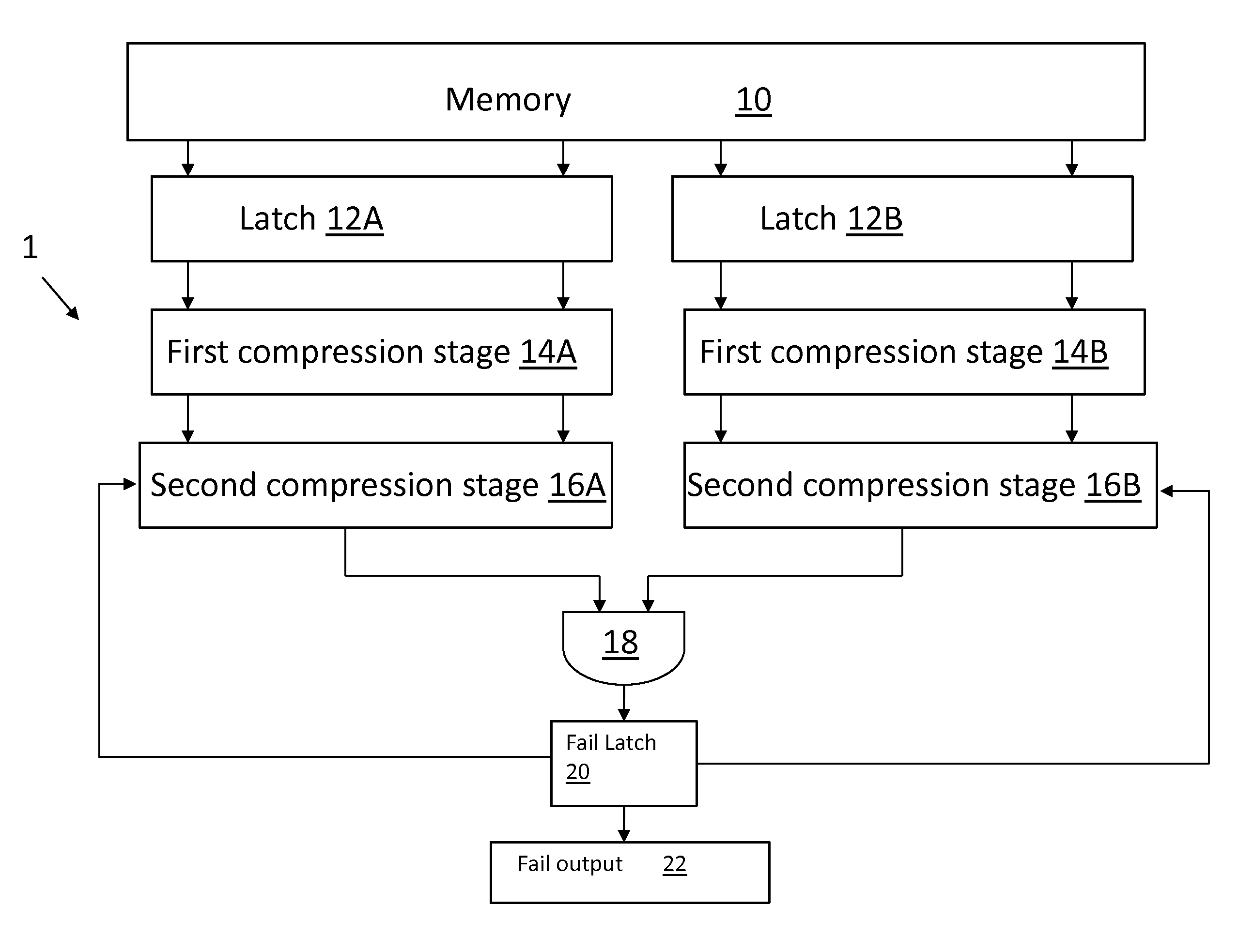
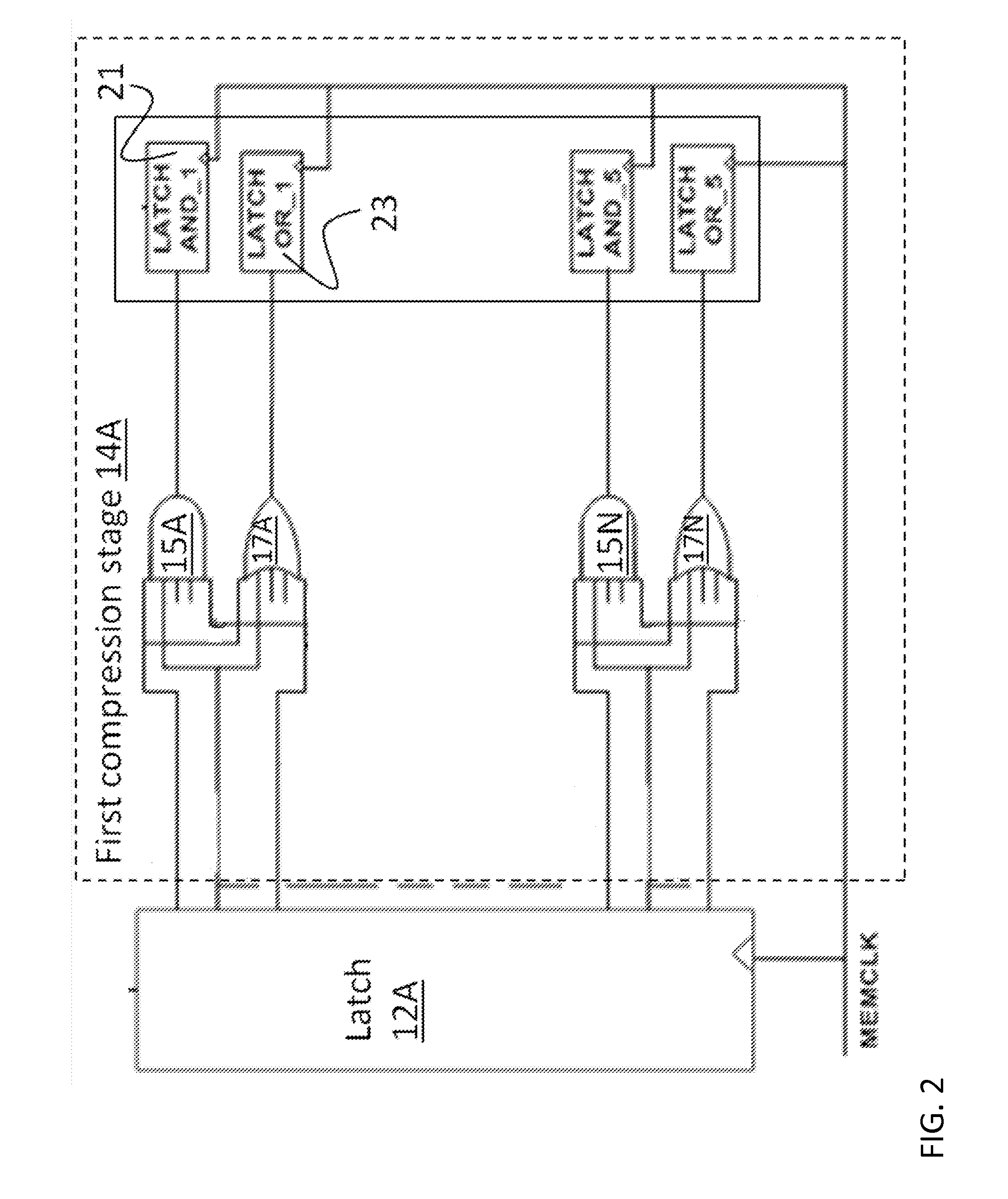
[0018]The subject matter disclosed herein relates generally to integrated circuits. More specifically, the disclosure provided herein relates to a method and architecture for reducing the test time of a built-in-self-test (BIST) for a memory of an integrated circuit (IC) chip.

[0019]Modern day digital signal processors, microprocessors, and network chips process lots of information and store the processed data into memory. Memory typically occupies almost half of the chip area. With decreasing technology nodes, more and more memory cells are closely packed together, thereby increasing the frequency and number of memory faults being detected. Each new technology gives rise to new fault models which require new sets of patterns to test the different kinds of faults in the memories. New patterns on top of legacy patterns from older technologies require more test time, thereby increasing the test cost and the cost of the chip.

[0020]A conventional BIST architecture tests the memory at-spe...


PUM


Abstract

Aspects of the invention provide for reducing BIST test time for a memory of an IC chip. In one embodiment, a BIST architecture for reducing BIST test time of a memory for an integrated circuit (IC) chip, the architecture comprising: a pair of latches for receiving bursts of data from a memory; a first compression stage for receiving a burst of data and compressing the burst of data into a plurality of latches; a second compression stage for comparing the compressed bursts of data with expected data; and a logic gate for determining whether there is a fail in the burst of data.

Description

FIELD OF THE INVENTION[0001]The subject matter disclosed herein relates generally to integrated circuits. More specifically, the disclosure provided herein relates to a method and architecture for reducing the test time of a built-in-self-test (BIST) for a memory of an integrated circuit (IC) chip.BACKGROUND OF THE INVENTION[0002]Modern day digital signal processors, microprocessors, and network chips process lots of information and store the processed data into memory. Memory typically occupies almost half of the chip area. With decreasing technology nodes, more and more memory cells are closely packed together, thereby increasing the frequency and number of memory faults being detected. Each new technology gives rise to new fault models which require new sets of patterns to test the different kinds of faults in the memories. These new sets of patterns which may be added on top of legacy patterns from older technologies, require more test time, thereby increasing the test cost and ...

Claims


Application Information

Patent Timeline
IPC IPC(8): G11C29/40
CPCG11C29/40G01R31/31703G01R31/318547
Inventor GORMAN, KEVIN W.HANAGANDI, DEEPAK I.MONDAL, KRISHNENDUOUELLETTE, MICHAEL R.
Owner IBM CORP
Why Eureka
Try Eureka