Apparatus and methods for pulsed photo-excited deposition and etch
- Summary
- Abstract
- Description
- Claims
- Application Information
AI Technical Summary
Benefits of technology
Problems solved by technology
Method used
Image
Examples
Embodiment Construction
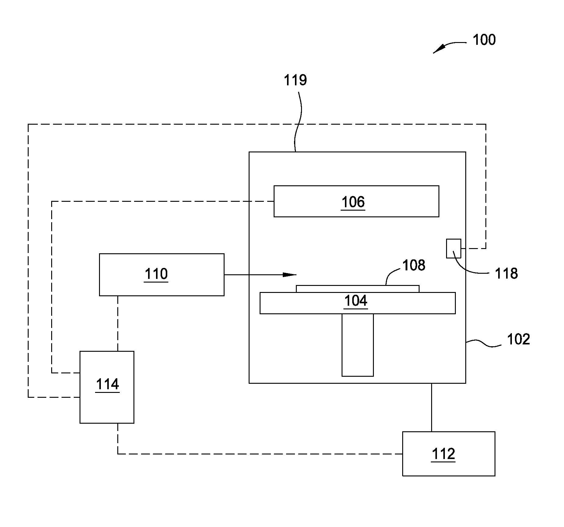
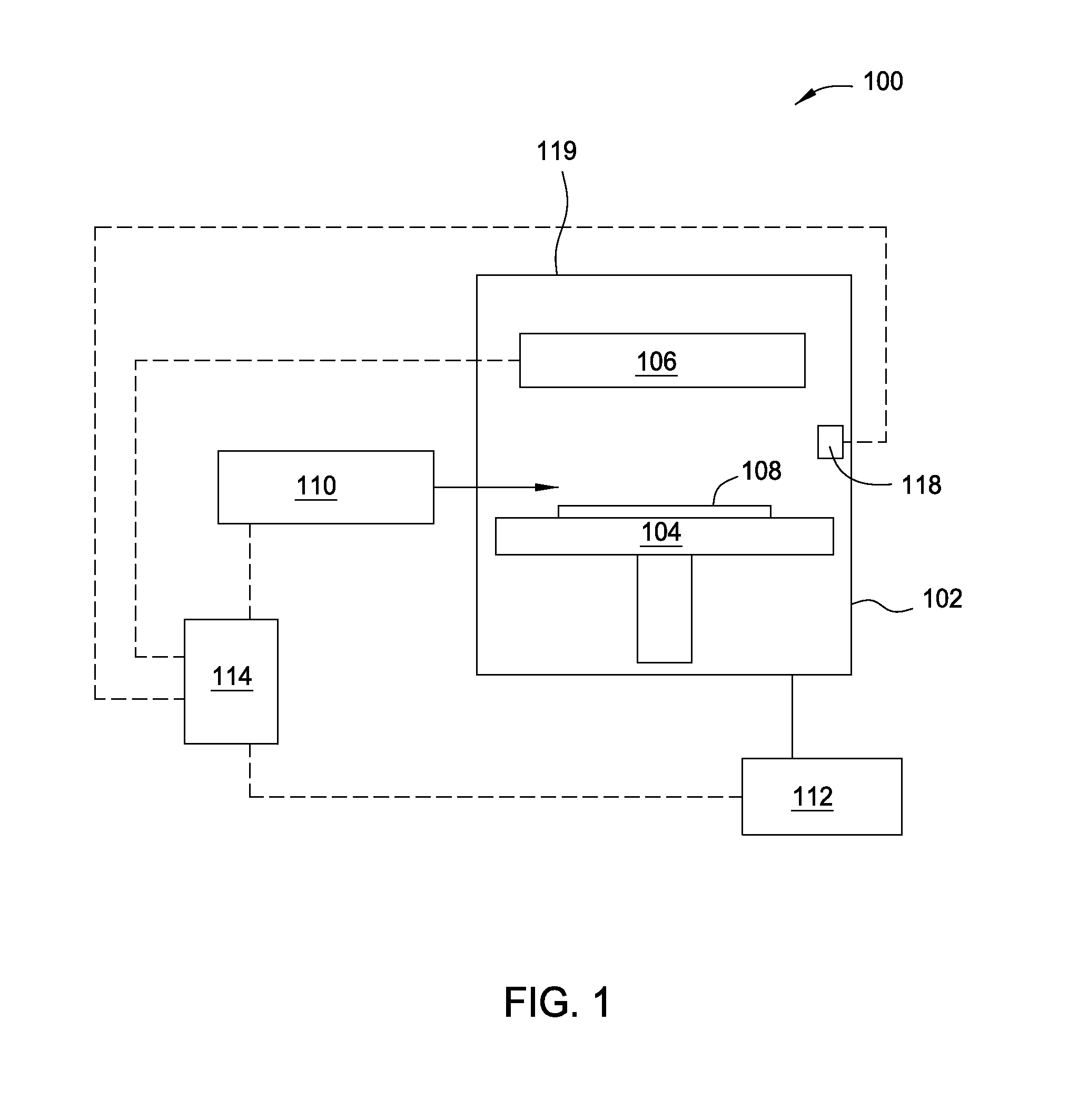
[0013]FIG. 1 illustrates a schematic sectional view of an exemplary thermal processing chamber 100 that may be used to practice embodiments of the present invention. As will be discussed below, the thermal processing system 100 has a pulsed radiation source that can be used to rapidly, selectively assist or excite precursor gases in a low pressure chamber disposed within the thermal processing system 100 for either deposition or etch process without changing the precursor gases and related transitions, as would otherwise required by the conventional approach if the deposition and etch processes are involved within the same chamber. It is contemplated that the present invention is not limited to the configuration of the processing chamber 100 as shown since the concept of the present invention may also be utilized in other processing chambers such as a chemical vapor deposition (CVD) chamber, an atomic layer deposition (ALD) chamber, or an atomic layer epitaxy (ALE) chamber where etc...
PUM
| Property | Measurement | Unit |
|---|---|---|
| Time | aaaaa | aaaaa |
| Wavelength | aaaaa | aaaaa |
| Wavelength | aaaaa | aaaaa |
Abstract
Description
Claims
Application Information


