Through-Silicon Vias and Interposers Formed by Metal-Catalyzed Wet Etching

a technology of wet etching and through-silicon vias, which is applied in the direction of semiconductor devices, semiconductor/solid-state device details, electrical devices, etc., can solve the problems of limited length scale studies, and achieve the effects of low cost, reduced thermal resistance, and low cos

Active Publication Date: 2014-09-18
X DISPLAY CO TECH LTD
View PDF4 Cites 9 Cited by
  • Summary
  • Abstract
  • Description
  • Claims
  • Application Information

AI Technical Summary

Benefits of technology

[0004]Provided herein are silicon interposers with through-vias that have substantially vertical sidewalls. Preferably, the methods and systems provided herein relate to through-vias having minimal or no porosity in the through-via side walls. Provided are low cost methods of forming through-vias in silicon with vertical sidewalls. Provided are low cost interposers with reduced thermal resistance and reduced thermal expansion. Provided is a low cost method of forming electrically useful high aspect ratio through-vias in silicon.

Problems solved by technology

That study, however, is limited in terms of length scales and fundamentally relates to porous materials.

Method used


Image

  • Through-Silicon Vias and Interposers Formed by Metal-Catalyzed Wet Etching
  • Through-Silicon Vias and Interposers Formed by Metal-Catalyzed Wet Etching
  • Through-Silicon Vias and Interposers Formed by Metal-Catalyzed Wet Etching

Examples


Embodiment Construction

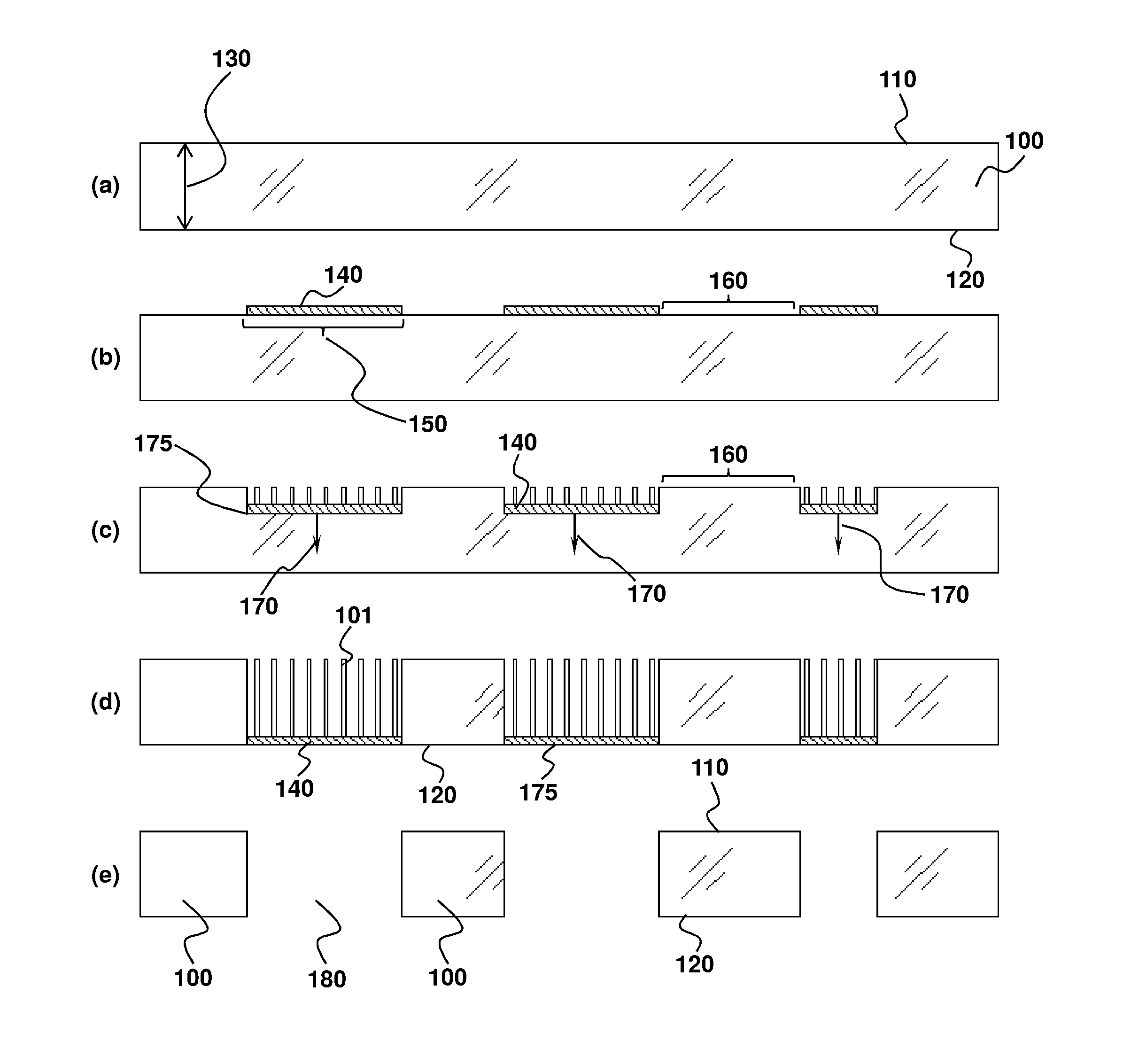
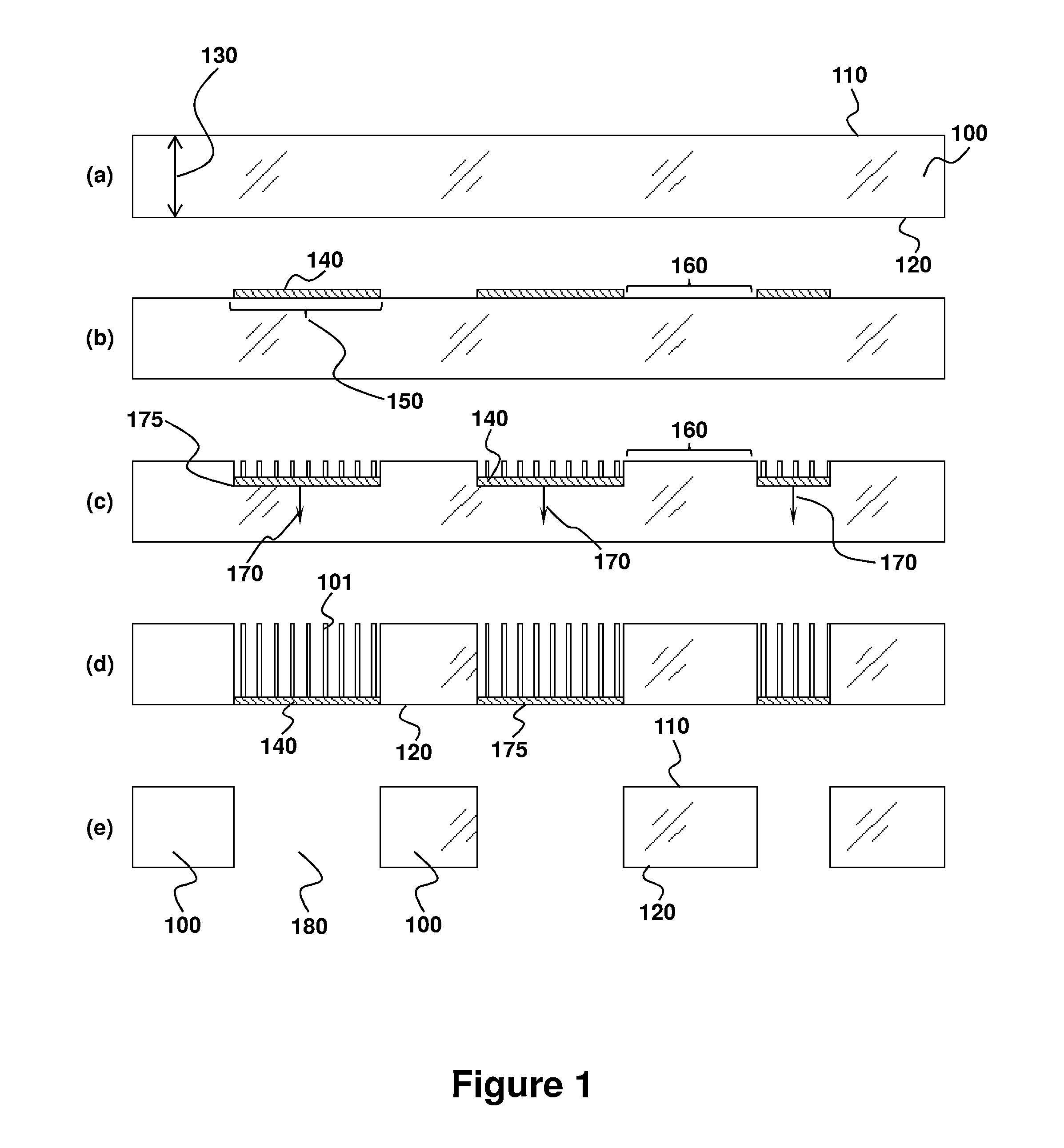
[0054]In general, the terms and phrases used herein have their art-recognized meaning, which can be found by reference to standard texts, journal references and contexts known to those skilled in the art. The following definitions are provided to clarify their specific use in the context of the invention.

[0055]“Noble metal structure” refers broadly to a noble metal that is provided on a top surface of the silicon substrate, such as a support surface. The outer shape of the structure corresponds to the shape of the through-via or recess feature that will be etched. The structure may be formed on the surface by any method known in the art, including by deposition, chemical vapor deposition, shadow mask deposition, photolithography, electrodeposition, lift-off or other transfer process. Alternatively, the structure may be preformed and transferred to the support surface, such as by a transfer printing process or selected deposition. For example, the noble metal structure may comprises ...


PUM

PropertyMeasurementUnit
diameteraaaaaaaaaa
opening sizeaaaaaaaaaa
thicknessaaaaaaaaaa

Abstract

Provided are methods for making a through-silicon via feature in a silicon substrate and related systems, such as by forming a noble metal structure on a silicon substrate support surface to generate silicon substrate contact regions that are in contact with or proximate to the noble metal structure; exposing at least a portion of the silicon substrate support surface and noble metal structure to an etchant to preferentially etch the silicon substrate contact regions compared to silicon substrate non-contact regions until the etch front reaches the silicon substrate bottom surface.

Description

CROSS-REFERENCE TO RELATED APPLICATIONS[0001]This application claims the benefit of U.S. Provisional Application No. 61 / 788,452, filed Mar. 15, 2013, which is specifically incorporated by reference to the extent not inconsistent herewith.BACKGROUND OF INVENTION[0002]The field of the invention is wafer level packaging on silicon substrates. More specifically, the field of the invention is wafer level packaging that uses through-silicon vias. In a preferred embodiment, the field of the invention is wafer level packaging for the production of sub-receivers and receivers for concentrator photovoltaic modules.[0003]Metal-assisted chemical etching is known in the art for forming nanostructures in silicon by highly anisotropic etching. Examples include US Pat. Pub. Nos. 2011 / 0263119, 2013 / 0052762; U.S. Pat. Nos. 6,762,134, 6,790,785; Huang et al. Adv. Mater. 2011, 23, 285-309; Peng et al. Adv. Funct. Mater. 2008, 18, 3026-3035; Appl. Phys. Lett. 77(16) (2000): 2572-2574. US Pat. Pub. No. 2...

Claims


Application Information

Patent Timeline
Patent Type & Authority Applications(United States)
IPC IPC(8): H01L21/768H01L23/498
CPCH01L23/49827H01L21/76898H01L21/30604H01L21/3081H01L23/147H01L23/49838H01L23/49872H01L2924/0002
Inventor MEITL, MATTHEWBOWER, CHRISTOPHER
Owner X DISPLAY CO TECH LTD
Why Eureka
Try Eureka